Max9489 multiple-output network clock generator – Rainbow Electronics MAX9489 User Manual
Page 2
MAX9489
Multiple-Output Network Clock Generator
2
_______________________________________________________________________________________
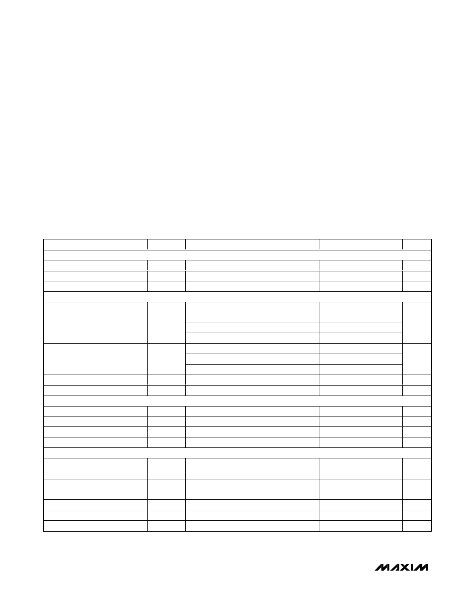
ABSOLUTE MAXIMUM RATINGS
DC ELECTRICAL CHARACTERISTICS
(V
DD
= AV
DD
= +3.0V to +3.6V, T
A
= -40°C to +85°C, unless otherwise noted. Typical values are at V
DD
= AV
DD
= +3.3V, T
A
= +25°C.)
(Note 1)
Stresses beyond those listed under “Absolute Maximum Ratings” may cause permanent damage to the device. These are stress ratings only, and functional
operation of the device at these or any other conditions beyond those indicated in the operational sections of the specifications is not implied. Exposure to
absolute maximum rating conditions for extended periods may affect device reliability.
V
DD
to GND ..............................................…….….-0.3V to +4.0V
AGND to GND .............................................……...-0.3V to +0.3V
All Other Pins to GND.................................-0.3V to (V
DD
+ 0.3V)
Short-Circuit Duration for all CLK_ Outputs ...............Continuous
Continuous Power Dissipation (T
A
= +70°C)
32-Pin Thin QFN (derate 21.3mW/°C above +70°C) ....1702mW
Storage Temperature Range .............................-65°C to +150°C
Maximum Junction Temperature .....................................+150°C
Operating Temperature Range ...........................-40°C to +85°C
ESD Rating (Human Body Model) .......................................±2kV
Lead Temperature (soldering, 10s) .................................+300°C
PARAMETER
SYMBOL
CONDITIONS
MIN
TYP
MAX
UNITS
CLOCK INPUT (X1)
Input High Level
V
IH1
2.0
V
Input Low Level
V
IL1
0.8
V
Input Current
I
IL1
, I
IH1
V
X
_ = 0 to V
DD
-5
+5
µA
CLOCK OUTPUTS (CLK_)
I
OH
= -100µA
V
DD
-
0.2
I
OH
= -4mA
2.4
Output High Level
V
OH
I
OH
= -8mA
2.1
V
I
OL
= 100µA
0.2
I
OL
= 4mA
0.4
Output Low Level
V
OL
I
OL
= 8mA
0.75
V
Output Short-Circuit Current
I
OS
CLK_ = V
DD
or GND
45
mA
Output Capacitance
C
O
(Note 2)
5
pF
TRI-LEVEL INPUTS (SEL, SA0, SA1)
Input High Level
V
IH2
2.5
V
Input Low Level
V
IL2
0.8
V
Input Open Level
V
IO2
1.35
1.90
V
Input Current
I
IL2
, I
IH2
V
IL2
= 0 or V
IH2
= V
DD
-10
+10
µA
SERIAL INTERFACE (SCL, SDA) (Note 3)
Input High Level
V
IH
0.7 x
V
DD
V
DD
V
Input Low Level
V
IL
0
0.3 x
V
DD
V
Input leakage Current
I
IH
, I
IL
-1
+1
µA
Low-Level Output
V
OL
I
SINK
= 4mA
0
0.4
V
Input Capacitance
Ci
(Note 2)
10
pF