Max9489 multiple-output network clock generator, Pin description – Rainbow Electronics MAX9489 User Manual
Page 6
MAX9489
Multiple-Output Network Clock Generator
6
_______________________________________________________________________________________
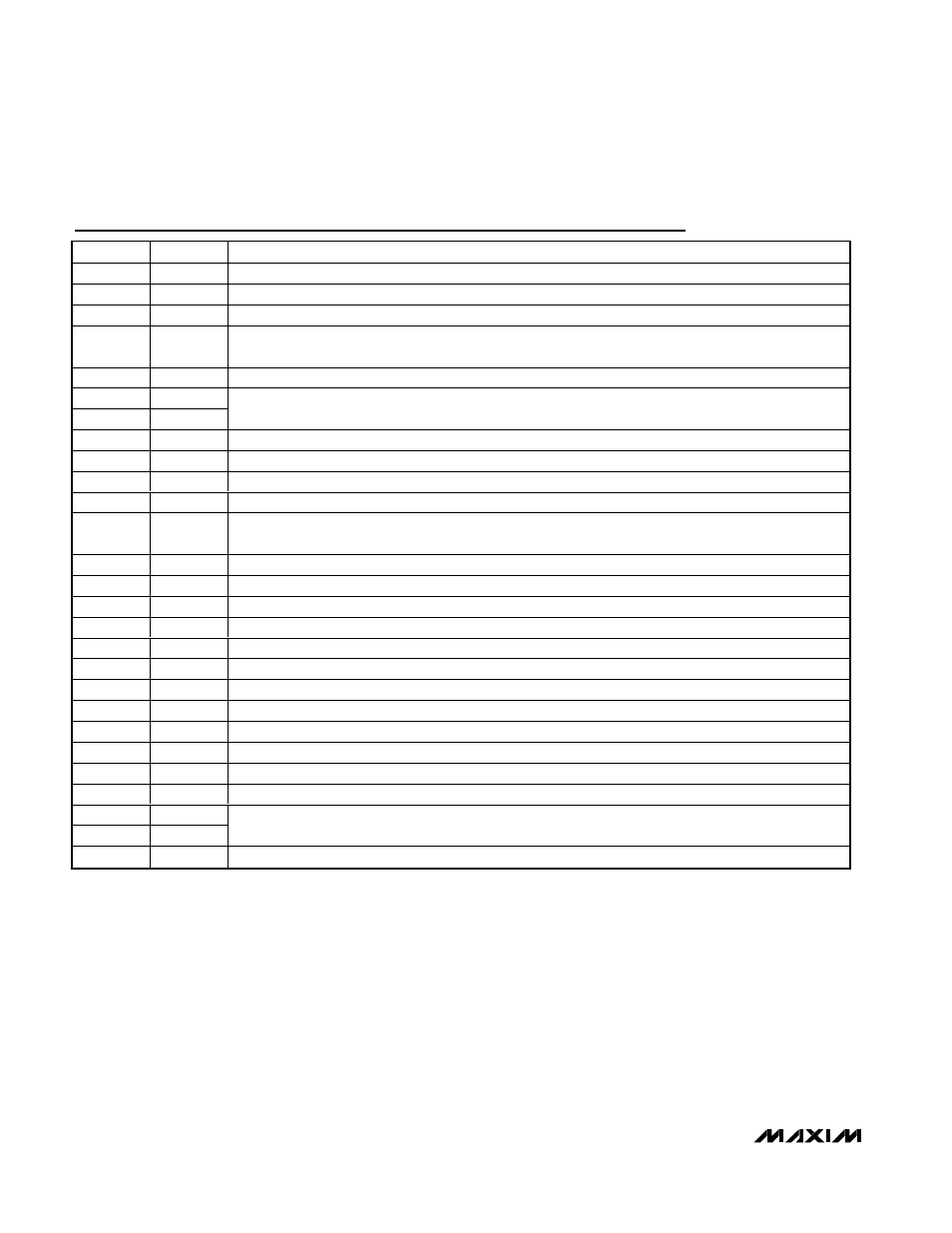
PIN
NAME
FUNCTION
1, 29
GND
Digital Ground
2
SCL
Serial Clock Input. Serial interface clock.
3
SDA
Serial Data I/O. Data I/O of serial interface.
4
SEL
Frequency Select for CLK1. Selects the frequency for CLK1 at power-up. SEL is a tri-level input. Force
SEL high for CLK1 = 100MHz. Leave SEL open for CLK1 = 125MHz. Force SEL low for CLK1 = 133MHz.
5
AV
DD
Power-Supply Input for Analog Circuits
6
X1
7
X2
Crystal Connection or Clock Input. If using a 25MHz crystal, connect it to X1 and X2. If using a reference
clock, connect the clock signal to X1, and leave X2 floating. See the Typical Operating Circuit.
8
AGND
Analog GND
9
CLK1
Clock 1 Output
10
CLK2
Clock 2 Output
11
CLK3
Clock 3 Output
12, 16, 20,
24, 28, 32
V
DD
Power-Supply Input for Digital Circuits
13
CLK4
Clock 4 Output
14
CLK5
Clock 5 Output
15
CLK6
Clock 6 Output
17
CLK7
Clock 7 Output
18
CLK8
Clock 8 Output
19
CLK9
Clock 9 Output
21
CLK10
Clock 10 Output
22
CLK11
Clock 11 Output
23
CLK12
Clock 12 Output
25
CLK13
Clock 13 Output
26
CLK14
Clock 14 Output
27
CLK15
Clock 15 Output
30
SA0
31
SA1
Address-Select Inputs for Serial Interface. SA0 and SA1 select the serial interface address, as shown in
Table 1. SA0 and SA1 are tri-level inputs, making nine possible address combinations.
EP
—
Exposed pad. Connect to GND.
Pin Description