Max9489 multiple-output network clock generator, Detailed description – Rainbow Electronics MAX9489 User Manual
Page 7
MAX9489
Multiple-Output Network Clock Generator
_______________________________________________________________________________________
7
Detailed Description
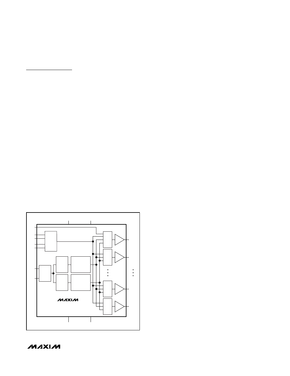
The MAX9489 clock generator produces 15 clock sig-
nals, CLK1 through CLK15. Each output is programma-
ble through control registers to any of 10 individual
frequencies: 133MHz, 125MHz, 100MHz, 83MHz,
80MHz, 66MHz, 62.5MHz, 50MHz, 33MHz, or 25MHz.
Additionally, the frequency of all outputs can be
changed ±5% or ±10% through the frequency-margin
control register. At power-up, the frequency of CLK1 is
pin programmable to 100MHz, 125MHz, or 133MHz,
and all other CLK outputs are logic low. The required
25MHz input reference frequency can be either a crys-
tal or an external clock signal. Figure 1 shows the
MAX9489 functional block diagram.
The MAX9489 is programmed through its I
2
C serial
interface. The I
2
C address is selected with two, tri-level
inputs, allowing up to nine MAX9489 devices to share
the same I
2
C bus. Power-supply and logic interface
signals are +3.0V to +3.6V. The operating state of the
MAX9489 is set by writing to the control registers, and
read by reading the control registers.
Reference Frequency Input
A reference frequency is required for the MAX9489.
The reference can be a 25MHz crystal or an external
clock signal. If using a 25MHz crystal, connect it across
X1 and X2, and connect 10pF capacitors from X1 and
X2 to GND (see the Typical Operating Circuit). If using
an external clock, connect the signal to X1 and leave
X2 floating.
Serial Interface
The MAX9489 is programmed through its I
2
C serial
interface. This interface has a clock, SCL, and a bidi-
rectional data line, SDA. In an I
2
C system, a master,
typically a microcontroller, initiates all data transfers to
and from slave devices, and generates the clock to
synchronize the data transfers.
The MAX9489 operates as a slave device. The timing of
the SDA and SCL signals is detailed in Figure 2, the
Serial Interface Timing diagram. SDA operates as both
an input and an open-drain output. A pullup resistor,
typically 4.7k
Ω, is required on SDA. SCL operates only
as an input. A pullup resistor, typically 4.7k
Ω, is
required on SCL if there are multiple masters on the 2-
wire bus, or if the master in a single-master system has
an open-drain SCL output.
Bit Transfer
One data bit is transferred during each SCL clock
cycle. SDA must remain stable during the high period
of SCL, because changes in SDA while SCL is high are
START and STOP control signals. Both SDA and SCL
idle high.
START and STOP Conditions
A master signals the beginning of a transmission with a
START condition by transitioning SDA from high to low
while SCL is high (Figure 2). When communication is
complete, a master issues a STOP condition by transi-
tioning SDA from low to high while SCL is high. The bus
is then free for another transmission.
Acknowledge Bits
After each 8 bits transferred, the receiving device gen-
erates an acknowledge signal by pulling SDA low for
the entire duration of the 9th clock pulse. If the receiv-
ing device does not pull SDA low, a not-acknowledge is
indicated (Figure 3).
Device Address
The MAX9489 has a 7-bit device address, pin config-
ured by the two tri-level address inputs SA1 and SA0.
To select the device address, connect SA1 and SA0 to
V
DD
, GND, or leave open, as indicated in Table 1. The
MAX9489 has nine possible addresses, allowing up to
nine MAX9489 devices to share the same interface bus.
MAX9489
MUX
CLK1
MUX
CLK2
MUX
CLK14
MUX
CLK15
400MHz
PLL1
25MHz
OSC
DIVIDE BY
3, 4, 5, 6, 12
400MHz
PLL2
DIVIDE BY
2, 3, 4, 5, 10
X1
X2
I
2
C
SDA
SCL
SEL
SA1
SA0
AV
DD
V
DD
AGND
GND
Figure 1. MAX9489 Functional Diagram