Rainbow Electronics MAX5965B User Manual
Page 2
MAX5965A/MAX5965B
High-Power, Quad, Monolithic, PSE Controllers
for Power over Ethernet
2
_______________________________________________________________________________________
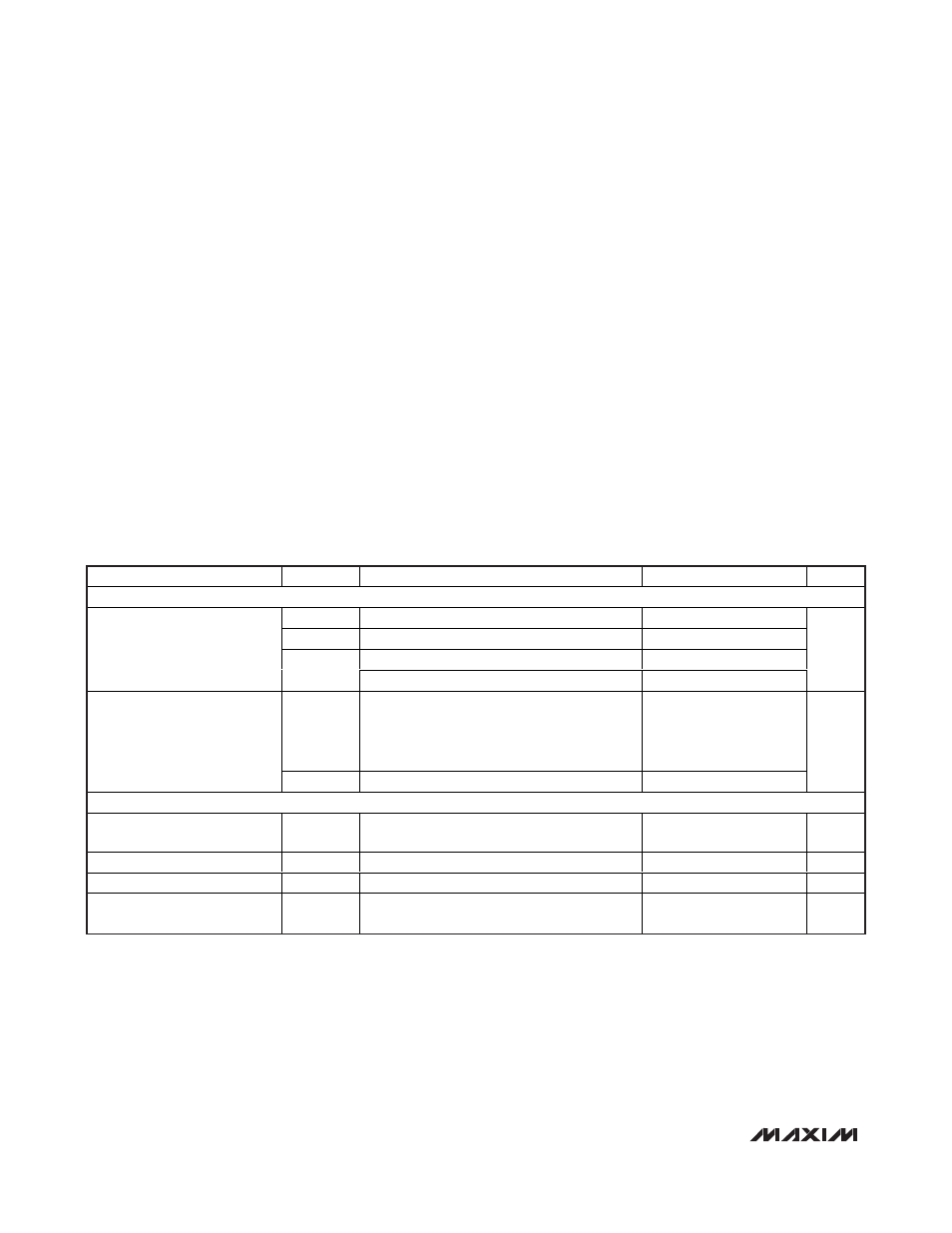
ABSOLUTE MAXIMUM RATINGS
ELECTRICAL CHARACTERISTICS
(V
AGND
= 32V to 60V, V
EE
= 0V, V
DD
to V
DGND
= +3.3V, all voltages are referenced to V
EE
, unless otherwise noted. Typical values are at
V
AGND
= +48V, V
DGND
= +48V, V
DD
= (V
DGND
+ 3.3V), T
A
= +25°C. Currents are positive when entering the pin and negative other-
wise.) (Note 2)
Stresses beyond those listed under “Absolute Maximum Ratings” may cause permanent damage to the device. These are stress ratings only, and functional
operation of the device at these or any other conditions beyond those indicated in the operational sections of the specifications is not implied. Exposure to
absolute maximum rating conditions for extended periods may affect device reliability.
(Voltages referenced to V
EE
, unless otherwise noted.)
AGND, DGND, DET_, V
DD
, RESET, A3–A0, SHD_, OSC,
SCL, SDAIN, AUTO .............................................-0.3V to +80V
OUT_........................................................-12V to (AGND + 0.3V)
GATE_ (internally clamped) (Note 1) ..................-0.3V to +11.4V
SENSE_ ..................................................................-0.3V to +24V
V
DD
, RESET, MIDSPAN, A3–A0, SHD_, OSC, SCL,
SDAIN and AUTO to DGND ..................................-0.3V to +7V
INT and SDAOUT to DGND....................................-0.3V to +12V
Maximum Current into INT, SDAOUT, DET_ .......................80mA
Maximum Power Dissipation (T
A
= +70°C)
36-Pin SSOP (derate 17.4mW/°C above +70°C) .....1388.9mW
Operating Temperature Ranges:
MAX5965A/MAX5965B_EAX ...…………………-40°C to +85°C
MAX5965A/MAX5965B_UAX ...............................0°C to +85°C
Storage Temperature Range .............................-65°C to +150°C
Junction Temperature ......................................................+150°C
Lead Temperature (soldering, 10s) .................................+300°C
Note 1: GATE_ is internally clamped to 11.4V above V
EE
. Driving GATE_ higher than 11.4V above V
EE
may damage the device.
PARAMETER
SYMBOL
CONDITIONS
MIN
TYP
MAX
UNITS
POWER SUPPLIES
V
AGND
V
AGND
- V
EE
32
60
V
DGND
0
60
V
DD
to V
DGND
, V
DGND
= V
AGND
2.4
3.6
Operating Voltage Range
V
DD
V
DD
to V
DGND
, V
DGND
= V
EE
3.0
3.6
V
I
EE
V
OUT_
= V
EE
, V
SENSE
_ = V
EE
, DET
_
= AGND,
all logic inputs open, SCL = SDAIN = V
DD
.
INT and SDAOUT unconnected. Measured at
AGND in power mode after GATE_ pullup
4.8
6.8
Supply Currents
I
DIG
All logic inputs high, measured at V
DD
0.2
0.4
mA
GATE DRIVER AND CLAMPING
GATE_ Pullup Current
I
PU
Power mode, gate drive on, V
GATE
= V
EE
(Note 3)
-40
-50
-65
µA
Weak GATE_ Pulldown Current
I
PDW
SHD_ = DGND, V
GATE_
= V
EE
+ 10V
42
µA
Maximum Pulldown Current
I
PDS
V
SENSE
= 600mV, V
GATE_
= V
EE
+ 2V
100
mA
External Gate Drive
V
GS
V
GATE
- V
EE
, power mode, gate drive on,
I
PU
= 1µA
9
10
11.5
V