C control channel, Typical operating characteristics, Max9258 ac electrical characteristics (continued) – Rainbow Electronics MAX9258 User Manual
Page 8
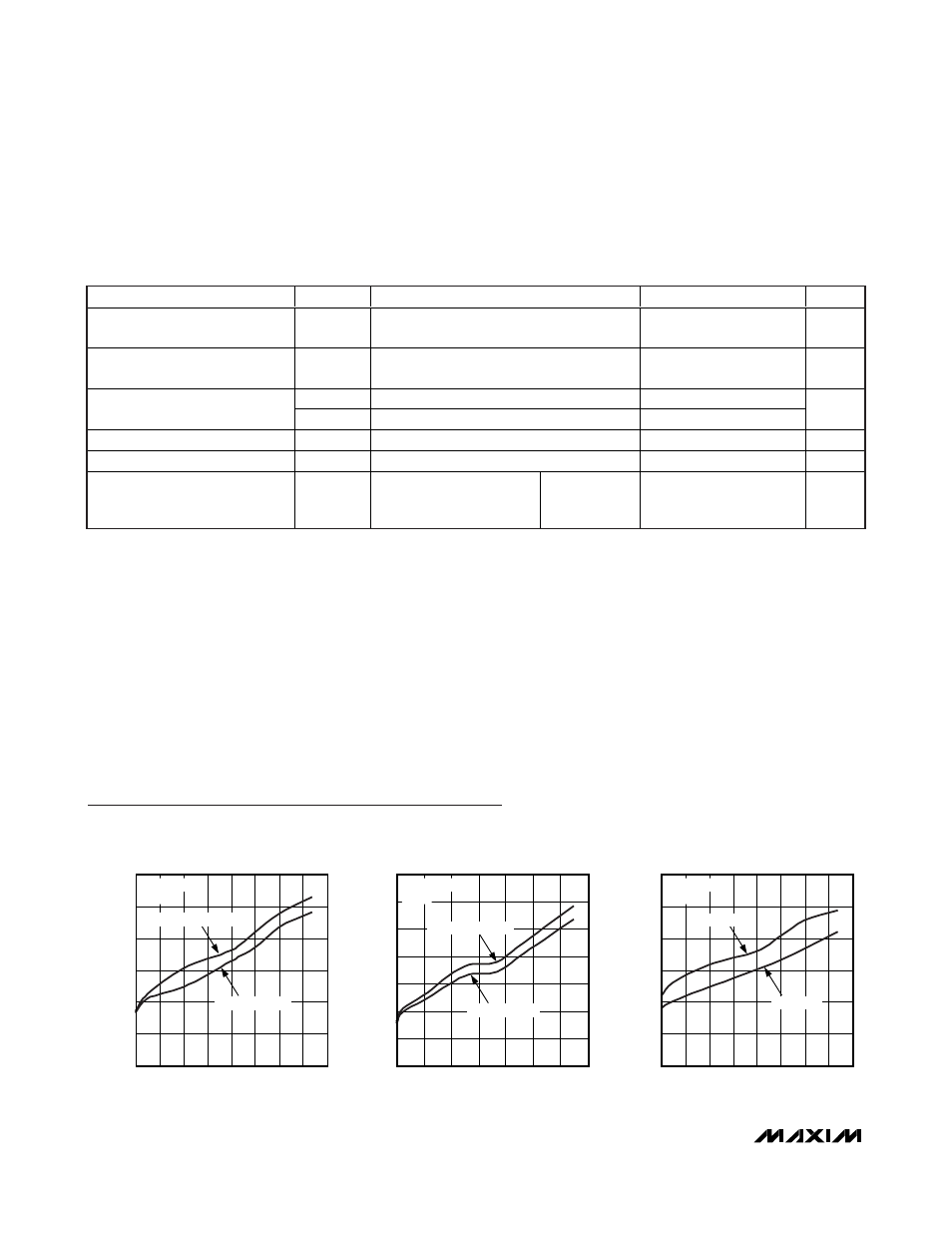
MAX9257 SUPPLY CURRENT
vs. FREQUENCY
MAX9257/58 toc01
PCLK FREQUENCY (MHz)
SUPPLY CURRENT (mA)
20
40
25
35
15
30
10
20
40
60
80
100
120
0
5
45
PRBS PATTERN
18-BIT
100% PREEMPHASIS
NO PREEMPHASIS
MAX9257 SUPPLY CURRENT
vs. FREQUENCY
MAX9257/58 toc02
PCLK FREQUENCY (MHz)
SUPPLY CURRENT (mA)
55
15
45
60
40
20
80
100
120
140
0
5
75
35
65
25
PRBS PATTERN
10-BIT
100% PREEMPHASIS
NO PREEMPHASIS
MAX9258 SUPPLY CURRENT
vs. FREQUENCY
MAX9257/58 toc03
PCLK FREQUENCY (MHz)
SUPPLY CURRENT (mA)
40
10
35
15
40
20
60
80
100
120
0
5
45
25
20
30
PRBS PATTERN
18-BIT
4% SPREAD
NO SPREAD
Typical Operating Characteristics
(V
CC_
= +3.3V, R
L
= 50Ω, C
L
= 8pF, T
A
= +25°C, unless otherwise noted.)
MAX9257/MAX9258
8
_______________________________________________________________________________________
Fully Programmable Serializer/Deserializer
with UART/I
2
C Control Channel
MAX9258 AC ELECTRICAL CHARACTERISTICS (continued)
V
CC_
= +3.0V to +3.6V, R
L
= 50Ω ±1%, C
L
= 8pF, differential input voltage |V
ID
| = 0.1V to 1.2V, input common-mode voltage
V
CM
= |V
ID
/2| to V
CC
- |V
ID
/2|, T
A
= -40°C to +105°C, unless otherwise noted. Typical values are at V
CC_
= +3.3V, |V
ID
| = 0.2V, V
CM
=
1.2V, T
A
= +25°C. (Notes 5, 6, and 7)
PARAMETER
SYMBOL
CONDITIONS
MIN
TYP
MAX
UNITS
Data Valid Before PCLK_ OUT
t
DVB
(Figure 11)
0.35 x
t
T
ns
Data Valid After PCLK_OUT
t
DVA
(Figure 11)
0.35 x
t
T
ns
t
SPD1
Spread off (Figure 14)
8t
T
Serial-to-Parallel Delay
t
SPD2
±4% spread
40t
T
ns
Power-Up Delay
t
PUD
(Figure 12)
100
ns
Power-Down to High Impedance
t
PDD
(Figure 13)
100
ns
Jitter Tolerance
t
JT
Each half of the UI, 12 bit,
SRATE = 840Mbps, PRBS
pattern (Figure 15)
No spread
0.25
0.30
UI
Note 2: Current into a pin is defined as positive. Current out of a pin is defined as negative. All voltages are referenced to ground
except V
TH
and VTL.
Note 3: Maximum and minimum limits over temperature are guaranteed by design and characterization. Devices are production
tested at T
A
= +105°C.
Note 4: One output at a time.
Note 5: AC parameters are guaranteed by design and characterization, and are not production tested.
Note 6: C
L
includes probe and test jig capacitance.
Note 7: t
T
is the period of the PCLK_OUT.
Note 8: For high-speed mode timing, see the
Detailed Description section.
Note 9: I
2
C timing parameters are specified for fast-mode I
2
C. Max data rate = 400kbps.