C control channel, Max9257 pin description – Rainbow Electronics MAX9258 User Manual
Page 10
MAX9257/MAX9258
10
______________________________________________________________________________________
Fully Programmable Serializer/Deserializer
with UART/I
2
C Control Channel
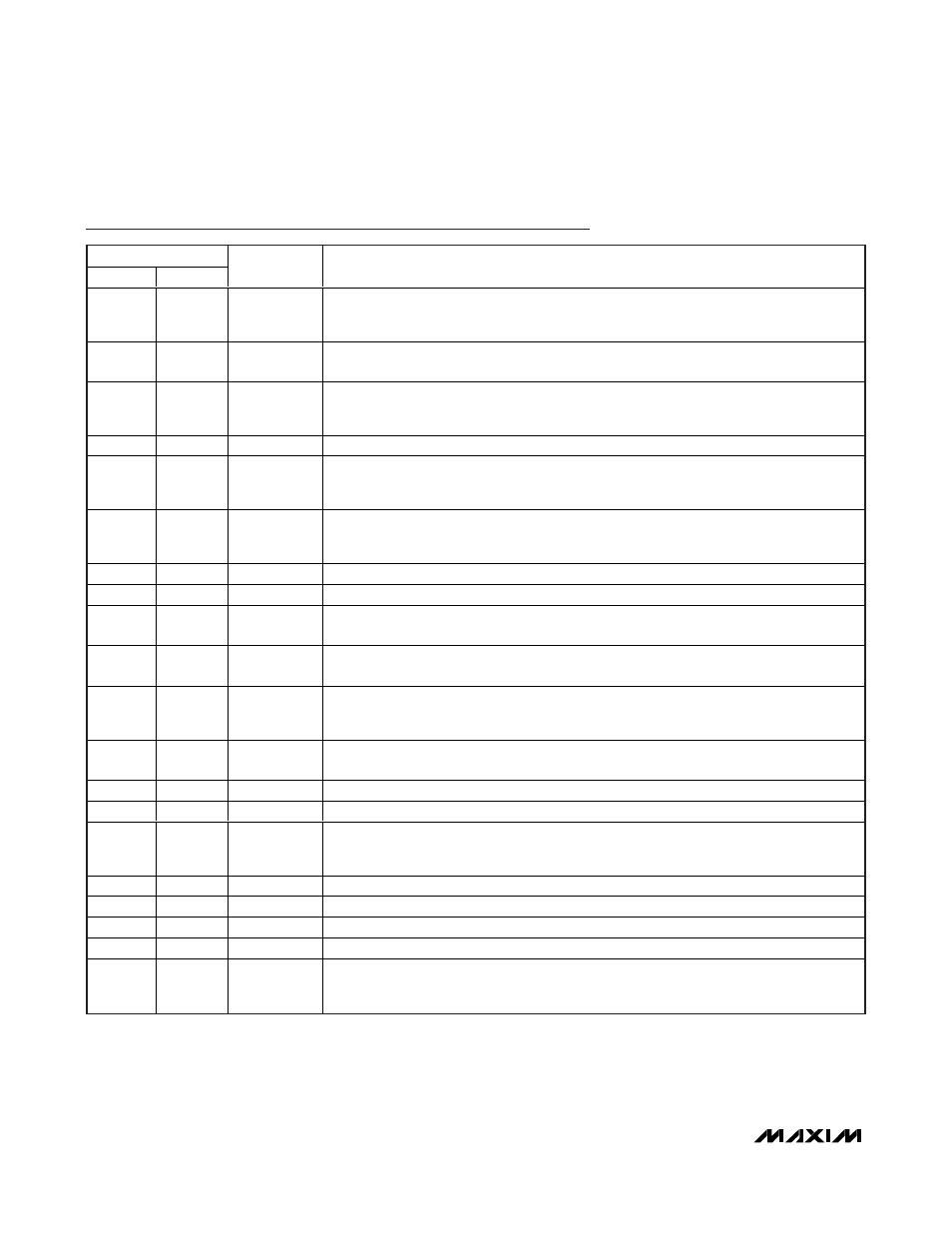
MAX9257 Pin Description
PIN
TQFN
LQFP
NAME
FUNCTION
1, 18
2, 21
V
CCIO
Single-Ended Input/Output Buffer Supply Voltage. Bypass V
CCIO
to GND with 0.1µF and
0.001µF capacitors in parallel as close as possible to the device with the smallest value
capacitor closest to V
CCIO
.
2, 11,
19, 34
3, 14,
22, 41
GND
Digital Supply Ground
3–8
4–9
DIN[9:14]/
GPIO[1:6]
Data Input/General Purpose Input/Output. When a serial-data word is less than 18 bits
word length, DIN_ not programmed as data inputs becomes GPIO (Table 22). DIN[9:14]
are internally pulled down to ground.
9
10
GND
FPLL
Filter PLL Ground
10
11
V
CCFPLL
Filter PLL Supply Voltage. Bypass V
CCFPLL
to GND
FPLL
with 0.1µF and 0.001µF capacitors
in parallel as close as possible to the device with the smallest value capacitor closest to
V
CCFPLL
.
12
15
DIN15/GPIO7
Data Input/General Purpose Input/Output. When a serial-data word is less than 18 bits
word length, DIN_ not programmed as data input becomes GPIO (Table 22). DIN15 is
internally pulled down to ground.
13
16
HSYNC_IN
Horizontal SYNC Input. HSYNC_IN is internally pulled down to ground.
14
17
VSYNC_IN
Vertical SYNC Input. VSYNC_IN is internally pulled down to ground.
15
18
PCLK_IN
Parallel Clock Input. PCLK_IN latches data and sync inputs and provides the PLL reference
clock. PCLK_IN is internally pulled down to ground.
16
19
SCL/TX
O p en- D r ai n C ontr ol C hannel Outp ut. S C L/TX b ecom es S C L outp ut w hen U ART- to- I
2
C i s
acti ve. S C L/TX b ecom es TX outp ut w hen U ART- to- I
2
C i s b yp assed . E xter nal l y p ul l up to V
C C
.
17
20
SDA/RX
Open-Drain Control Channel Input/Output. SDA/RX becomes bidirectional SDA when
UART-to-I
2
C is active. SDA/RX becomes RX input when UART-to-I
2
C is bypassed. SDA
output requires a pullup to V
CC
.
20, 33
23, 40
V
CC
Digital Supply Voltage. Bypass V
CC
to ground with 0.1µF and 0.001µF capacitors in p ar al l el
as cl ose as p ossi b l e to the d evi ce w i th the sm al l est val ue cap aci tor cl osest to V
C C
.
21
26
GPIO8
General Purpose Input/Output
22
27
GPIO9
General Purpose Input/Output
23
28
V
CCSPLL
Spread PLL Supply Voltage. Bypass V
CCSPLL
to GND
SPLL
with 0.1µF and 0.001µF
capacitors in parallel as close as possible to the device with the smallest value capacitor
closest to V
CCSPLL
.
24
29
GND
SPLL
SPLL Ground
25
30
GND
LVDS
LVDS Ground
26
31
SDO-
Serial LVDS Inverting Output
27
32
SDO+
Serial LVDS Noninverting Output
28
33
V
CCLVDS
LVDS Supply Voltage. Bypass V
CCLVDS
to GND
LVDS
with 0.1µF and 0.001µF capacitors in
parallel as close as possible to the device with the smallest value capacitor closest to
V
CCLVDS
.