C control channel, Max9257 pin description (continued), Max9258 pin description – Rainbow Electronics MAX9258 User Manual
Page 11
MAX9257/MAX9258
______________________________________________________________________________________
11
Fully Programmable Serializer/Deserializer
with UART/I
2
C Control Channel
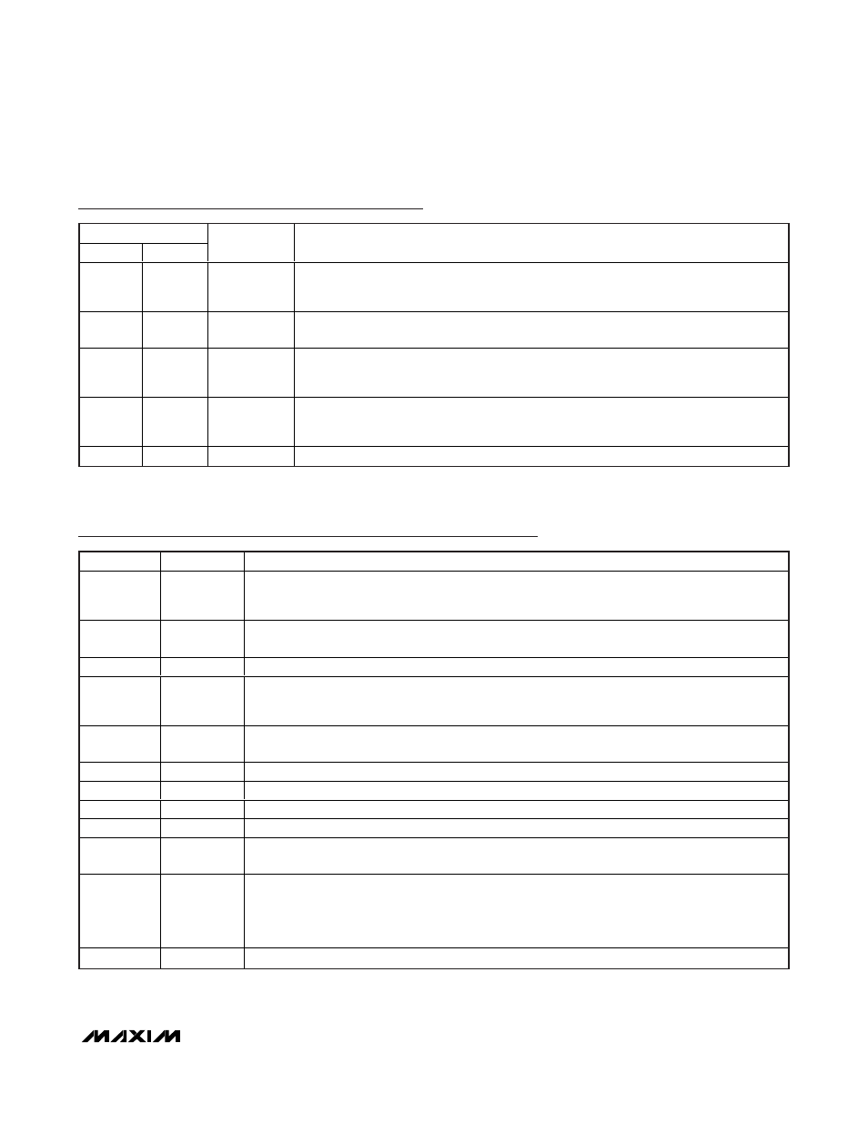
MAX9257 Pin Description (continued)
PIN
TQFN
LQFP
NAME
FUNCTION
29
34
REM
Remote Power-Up/Power-Down Select Input. Connect REM to ground for power-up to
follow V
CC
. Connect REM high to V
CC
through 10k
Ω resistor for remote power-up. REM is
internally pulled down to GND.
30, 31, 32,
35–39
35, 38,
39, 42–46
DIN[0:7]
Data Inputs. DIN[0:7] are internally pulled down to ground.
40
47
DIN8/GPIO0
Data Input/General Purpose Input/Output. When a serial-data word is less than 18 bits
word length, DIN_ not programmed as data input becomes GPIO (Table 22). DIN8 is
internally pulled down to ground.
—
1, 12, 13
24, 25,
36, 37, 48
N.C.
No Connection. Not internally connected.
—
—
EP
Exposed Pad for Thin QFN Package Only. Connect EP to ground.
MAX9258 Pin Description
PIN
NAME
FUNCTION
1, 12, 13, 24,
25, 36,
37
N.C.
No Connection. Not internally connected.
2
V
CC
Digital Supply Voltage. Bypass V
CC
to GND with 0.1µF and 0.001µF capacitors in parallel as close
as possible to the device with the smallest value capacitor closest V
CC
.
3, 14
GND
Digital Supply Ground
4
PD
LVCMOS/LVTTL Power-Down Input. Drive
PD high to power up the device and enable all outputs.
Drive
PD low to put all outputs in high impedance and reduce supply current. PD is internally pulled
down to ground.
5
V
CCLVDS
LVDS Supply Voltage. Bypass V
CCLVDS
to GND
LVDS
with 0.1µF and 0.001µF capacitors in parallel
as close as possible to the device with the smallest value capacitor closest to V
CCLVDS
.
6
SDI-
Serial LVDS Inverting Input
7
SDI+
Serial LVDS Noninverting Input
8
GND
LVDS
LVDS Supply Ground
9
GND
PLL
PLL Supply Ground
10
V
CCPLL
PLL Supply Voltage. Bypass V
CCPLL
to GND
PLL
with 0.1µF and 0.001µF capacitors in parallel as
close to the device as possible with the smallest value capacitor closest to V
CCPLL
.
11
ERROR
Active-Low, Open-Drain Error Output.
ERROR asserts low to indicate a data transfer error was
detected (parity, PRBS, or UART control channel error).
ERROR is high to indicate no error detected.
ERROR resets when the error registers are read for parity, control channel errors, and when PRBS
enable bit is reset for PRBS errors. Pull up to V
CCOUT
with a 1k
Ω resistor.
15
RX
LVCMOS/LVTTL Control Channel UART Output