14 reset timing, Figure 6-8. clock timing, Table 6-9. reset (xrs) timing requirements – Texas Instruments Digital Signal Processor SM320F2812-HT User Manual
Page 95
See Note A
See Note B
SGUS062B
–
JUNE 2009
–
REVISED JUNE 2011
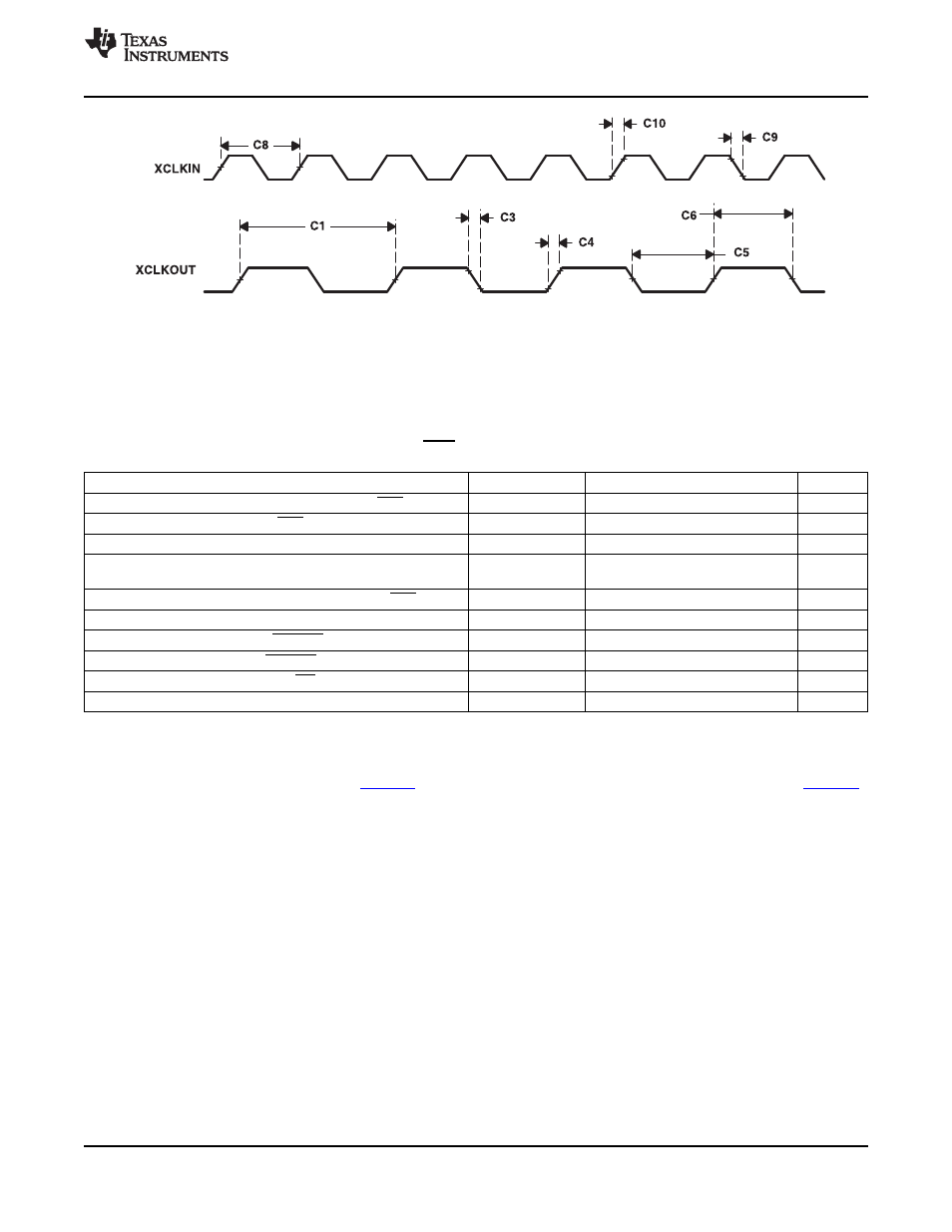
A.
The relationship of XCLKIN to XCLKOUT depends on the divide factor chosen. The waveform relationship shown in
is intended to illustrate the timing parameters only and may differ based on configuration.
B.
XCLKOUT configured to reflect SYSCLKOUT.
Figure 6-8. Clock Timing
6.14 Reset Timing
Table 6-9. Reset (XRS) Timing Requirements
(1) (2)
MIN
NOM
MAX
UNIT
t
w(RSL1)
Pulse duration, stable XCLKIN to XRS high
8t
c(CI)
cycles
t
w(RSL2)
Pulse duration, XRS low
Warm reset
8t
c(CI)
cycles
WD-initiated reset
512t
c(CI)
Pulse duration, reset pulse generated by
t
w(WDRS)
512t
c(CI)
cycles
watchdog
t
d(EX)
Delay time, address/data valid after XRS high
32t
c(CI)
cycles
t
OSCST
(3)
Oscillator start-up time
1
10
ms
t
su(XPLLDIS)
Setup time for XPLLDIS pin
16t
c(CI)
cycles
t
h(XPLLDIS)
Hold time for XPLLDIS pin
16t
c(CI)
cycles
t
h(XMP/MC)
Hold time for XMP/MC pin
16t
c(CI)
cycles
t
h(boot-mode)
Hold time for boot-mode pins
2520t
c(CI)
(4)
cycles
(1)
If external oscillator/clock source isused, reset time has to be low at least for 1 ms after V
DD
reaches 1.5 V.
(2)
Not production tested.
(3)
Dependent on crystal/resonator and board design.
(4)
The boot ROM reads the password locations. Therefore, this timing requirement includes the wakeup time for flash. See the
TMS320x281x Boot ROM Reference Guide (
) and TMS320x281x System Control and Interrupts Reference Guide
for further information.
Copyright
©
2009
–
2011, Texas Instruments Incorporated
Electrical Specifications
95
Product Folder Link(s):