3 die layout – Texas Instruments Digital Signal Processor SM320F2812-HT User Manual
Page 14
SGUS062B
–
JUNE 2009
–
REVISED JUNE 2011
2.3
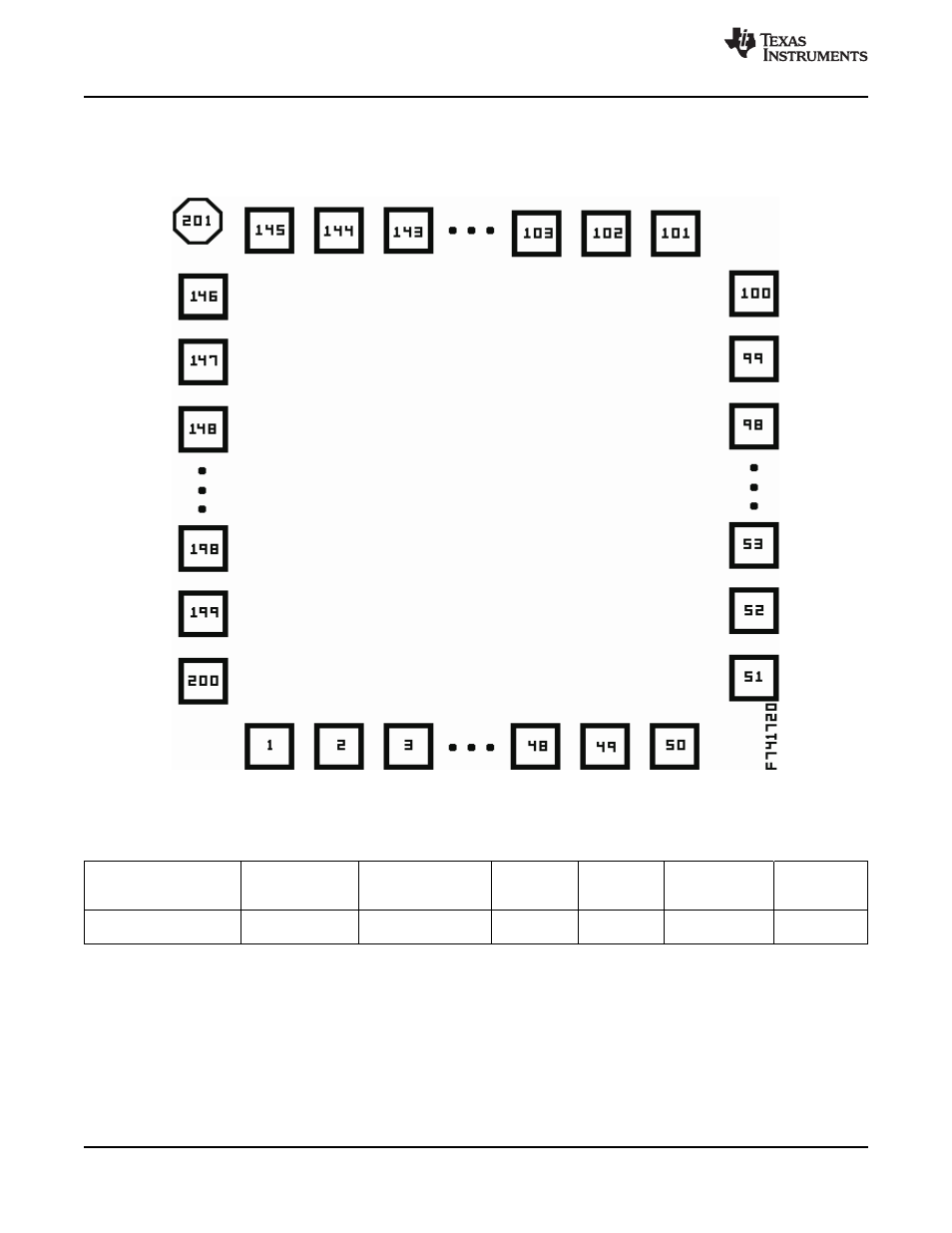
Die Layout
The SM320F2812 die layout is shown in
. See
for a description of each pad's
function.
Figure 2-1. SM320F2812 Die Layout
Table 2-2. Bare Die Information
DIE PAD
DIE PAD
DIE
BACKSIDE
BACKSIDE
DIE SIZE
DIE PAD SIZE
COMPOSITI
COORDINATES
THICKNESS
FINISH
POTENTIAL
ON
219.4 x 207.0 (mils);
Silicon with
55.0 x 64.0 (
μ
m)
See
11.0 mils
AlCu/TiN
Ground
5572.0 x 5258.0 (
μ
m)
backgrind
14
Introduction
Copyright
©
2009
–
2011, Texas Instruments Incorporated
Product Folder Link(s):
See also other documents in the category Texas Instruments Hardware:
- MSP430x1xx (440 pages)
- Laser And Motor Drives DRV8811EVM (13 pages)
- TMS320 DSP (88 pages)
- MSP430x11x1 (45 pages)
- TVP5154EVM (55 pages)
- TMS320DM646X DMSOC (64 pages)
- CC2511 (24 pages)
- SN65HVS880 (4 pages)
- TPS650231EVM (14 pages)
- TMS320TCI648x (256 pages)
- TSC2007EVM-PDK (16 pages)
- UCC38500EVM (16 pages)
- TMS320C6000 (62 pages)
- SCAU020 (21 pages)
- TPS40051 (17 pages)
- TNETE2201 (14 pages)
- TMS320C64x DSP (306 pages)
- UCC2891 (21 pages)
- TMS320C3x (757 pages)
- MSP430 (138 pages)
- TMS320C6712D (102 pages)
- MSP430x4xx (512 pages)
- TMS320C6454 (225 pages)
- SPRU938B (48 pages)
- TUSB3210 (22 pages)
- TMS320C6457 (43 pages)
- CC2530ZNP (3 pages)
- TMS320C6455 (50 pages)
- TSB12LV26 (91 pages)
- TMS320C6472 (2 pages)
- VLYNQ Port (49 pages)
- TMS380C26 (92 pages)
- MSP-FET430 (95 pages)
- TMS320TCI6486 (160 pages)
- TPS2330 (22 pages)
- DM648 DSP (47 pages)
- TMS320DM36X (134 pages)
- MSC1211 (35 pages)
- SPRAA56 (29 pages)
- DAC7741EVM (28 pages)
- CDCM7005 (34 pages)
- TMS370 (99 pages)
- Adpater (37 pages)
- TMS320C6452 DSP (46 pages)