Texas Instruments Digital Signal Processor SM320F2812-HT User Manual
Page 113
t
c(SPC)
+
SPI clock
cycle time
+
LSPCLK
4
or
LSPCLK
(SPIBRR
)
1)
+
t
c(LCO)
+
LSPCLK cycle time
(2)
SGUS062B
–
JUNE 2009
–
REVISED JUNE 2011
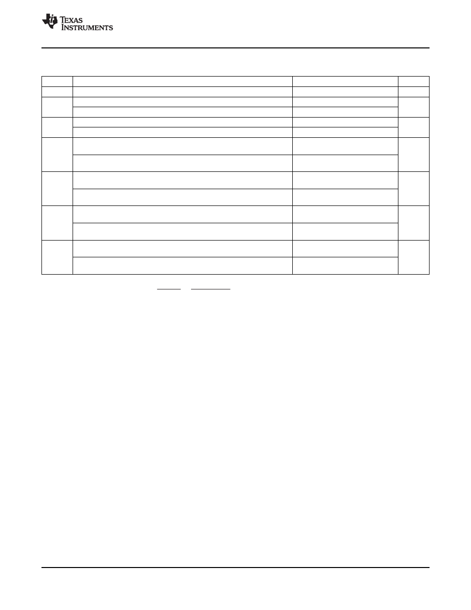
Table 6-24. SPI Slave Mode External Timing (Clock Phase = 1)
(1) (2) (3)
NO.
MIN
MAX
UNIT
12
t
c(SPC)S
Cycle time, SPICLK
8tc(LCO)
ns
t
w(SPCH)S
Pulse duration, SPICLK high (clock polarity = 0)
0.5t
c(SPC)S
–
10
0.5t
c(SPC)S
13
(4)
ns
t
w(SPCL)S
Pulse duration, SPICLK low (clock polarity = 1)
0.5t
c(SPC)S
–
10
0.5t
c(SPC)S
t
w(SPCL)S
Pulse duration, SPICLK low (clock polarity = 0)
0.5t
c(SPC)S
–
10
0.5t
c(SPC)S
14
(4)
ns
t
w(SPCH)S
Pulse duration, SPICLK high (clock polarity = 1)
0.5t
c(SPC)S
–
10
0.5t
c(SPC)S
Setup time, SPISOMI before SPICLK high
t
su(SOMI-SPCH)S
0.125t
c(SPC)S
(clock polarity = 0)
17
(4)
ns
Setup time, SPISOMI before SPICLK low
t
su(SOMI-SPCL)S
0.125t
c(SPC)S
(clock polarity = 1)
Valid time, SPIS OMI data valid after SPICLK high
t
v(SPCH-SOMI)S
0.75t
c(SPC)S
(clock polarity = 0)
18
(4)
ns
Valid time, SPISOMI data valid after SPICLK low
t
v(SPCL-SOMI)S
0.75t
c(SPC)S
(clock polarity = 1)
Setup time, SPISIMO before SPICLK high
t
su(SIMO-SPCH)S
0
(clock polarity = 0)
21
(5)
ns
Setup time, SPISIMO before SPICLK low
t
su(SIMO-SPCL)S
0
(clock polarity = 1)
Valid time, SPISIMO data valid after SPICLK high
tv
(SPCH-SIMO)S
0.5t
c(SPC)S
(clock polarity = 0)
22
(5)
ns
Valid time, SPISIMO data valid after SPICLK low
t
v(SPCL-SIMO)S
0.5t
c(SPC)S
(clock polarity = 1)
(1)
The MASTER/SLAVE bit (SPICTL.2) is cleared and the CLOCK PHASE bit (SPICTL.3) is set.
(3)
Not production tested.
(4)
The active edge of the SPICLK signal referenced is controlled by the CLOCK POLARITY bit (SPICCR.6).
(5)
The active edge of the SPICLK signal referenced is controlled by the CLOCK POLARITY bit (SPICCR.6).
Copyright
©
2009
–
2011, Texas Instruments Incorporated
Electrical Specifications
113
Product Folder Link(s):