3 functional overview, 3functional overview, Figure 3-1. functional block diagram – Texas Instruments Digital Signal Processor SM320F2812-HT User Manual
Page 25
M0 SARAM
1K x 16
CPU-Timer 0
CPU-Timer 1
INT[12:1]
CLKIN
Real-Time JTAG
CPU-Timer 2
Peripheral Bus
C28x CPU
H0 SARAM
8K ⋅ 16
INT14
NMI
INT13
Memory Bus
M1 SARAM
1K x 16
Flash
128K x 16
Boot ROM
4K ⋅ 16
eCAN
SCIA/SCIB
12-Bit ADC
External Interrupt
Control
(XINT1/2/13, XNMI)
EVA/EVB
Memory Bus
OTP
1K x 16
McBSP
System Control
(Oscillator and PLL
+
Peripheral Clocking
+
Low-Power
Modes
+
WatchDog)
FIFO
FIFO
PIE
(96 interrupts)
†
RS
SPI
FIFO
TINT0
TINT1
TINT2
Control
Address(19)
Data(16)
External
Interface
(XINTF)
16 Channels
†
45 of the possible 96 interrupts are used on the device.
GPIO Pins
XRS
X1/XCLKIN
X2
XF_XPLLDIS
Protected by the code-security module.
XINT13
G
P
I
O
M
U
X
L1 SARAM
4K x 16
XNMI
L0 SARAM
4K x 16
‡
‡
‡
‡
‡
SGUS062B
–
JUNE 2009
–
REVISED JUNE 2011
3
Functional Overview
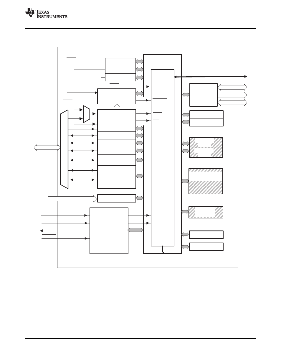
Figure 3-1. Functional Block Diagram
Copyright
©
2009
–
2011, Texas Instruments Incorporated
Functional Overview
25
Product Folder Link(s):
- MSP430x1xx (440 pages)
- Laser And Motor Drives DRV8811EVM (13 pages)
- TMS320 DSP (88 pages)
- MSP430x11x1 (45 pages)
- TVP5154EVM (55 pages)
- TMS320DM646X DMSOC (64 pages)
- CC2511 (24 pages)
- SN65HVS880 (4 pages)
- TPS650231EVM (14 pages)
- TMS320TCI648x (256 pages)
- TSC2007EVM-PDK (16 pages)
- UCC38500EVM (16 pages)
- TMS320C6000 (62 pages)
- SCAU020 (21 pages)
- TPS40051 (17 pages)
- TNETE2201 (14 pages)
- TMS320C64x DSP (306 pages)
- UCC2891 (21 pages)
- TMS320C3x (757 pages)
- MSP430 (138 pages)
- TMS320C6712D (102 pages)
- MSP430x4xx (512 pages)
- TMS320C6454 (225 pages)
- SPRU938B (48 pages)
- TUSB3210 (22 pages)
- TMS320C6457 (43 pages)
- CC2530ZNP (3 pages)
- TMS320C6455 (50 pages)
- TSB12LV26 (91 pages)
- TMS320C6472 (2 pages)
- VLYNQ Port (49 pages)
- TMS380C26 (92 pages)
- MSP-FET430 (95 pages)
- TMS320TCI6486 (160 pages)
- TPS2330 (22 pages)
- DM648 DSP (47 pages)
- TMS320DM36X (134 pages)
- MSC1211 (35 pages)
- SPRAA56 (29 pages)
- DAC7741EVM (28 pages)
- CDCM7005 (34 pages)
- TMS370 (99 pages)
- Adpater (37 pages)
- TMS320C6452 DSP (46 pages)