Texas Instruments Digital Signal Processor SM320F2812-HT User Manual
Page 60
ADCINA[7:0]
ADCINB[7:0]
ADCLO
ADCBGREFIN
†
ADC External Current Bias Resistor
ADCRESEXT
ADCREFP
V
DDA1
V
DDA2
V
SSA1
V
SSA2
AVDDREFBG
AVSSREFBG
V
DDAIO
V
SSAIO
V
DD1
V
SS1
Test Pin
ADC Reference Positive Output
ADCREFM
ADC Reference Medium Output
ADC Analog Power
ADC Reference Power
ADC Analog I/O Power
ADC Digital Power
Analog input 0−3 V with respect to ADCLO
Connect to Analog Ground
24.9 k
W
/20 k
W
(See Note C)
10
m
F
‡
10
m
F
‡
Analog 3.3 V
Analog 3.3 V
Analog 3.3 V
Analog 3.3 V
Analog Ground
1.8 V
ADCREFP and ADCREFM should not
be loaded by external circuitry
can use the same 1.8 V (or 1.9 V) supply as the
digital core but separate the two with a ferrite
bead or a filter
Digital Ground
ADC 16-Channel Analog Inputs
†
Provide access to this pin in PCB layouts. Intended for test purposes only.
‡
TAIYO YUDEN EMK325F106ZH, EMK325BJ106MD, or equivalent
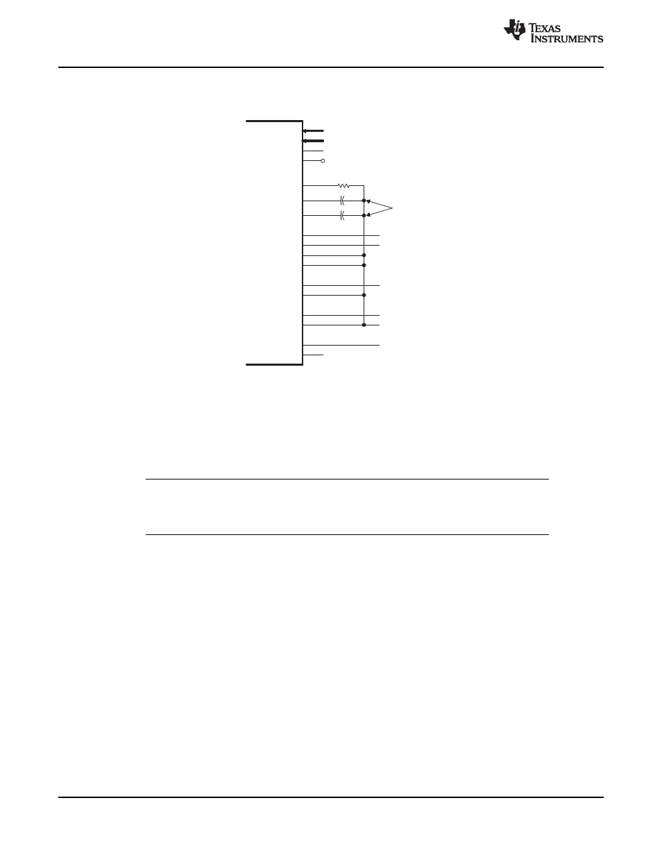
NOTES: A. External decoupling capacitors are recommended on all power pins.
B. Analog inputs must be driven from an operational amplifier that does not degrade the ADC performance.
C. Use 24.9 k
Ω
for ADC clock range 1 − 18.75 MHz; use 20 k
Ω
for ADC clock range 18.75 − 25 MHz.
SGUS062B
–
JUNE 2009
–
REVISED JUNE 2011
shows the ADC pin-biasing for internal reference and
shows the ADC pin-biasing for
external reference.
Figure 4-5. ADC Pin Connections With Internal Reference (See Notes A and B)
NOTE
The temperature rating of any recommended component must match the rating of the end
product.
60
Peripherals
Copyright
©
2009
–
2011, Texas Instruments Incorporated
Product Folder Link(s):