28 xhold/xholda timing, Figure 6-35. external interface hold waveform – Texas Instruments Digital Signal Processor SM320F2812-HT User Manual
Page 129
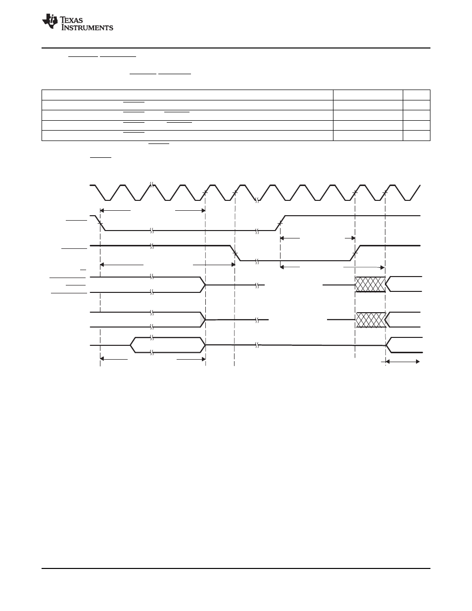
XCLKOUT
(/1 Mode)
XHOLD
XR/W,
XZCS0AND1,
XZCS2,
XZCS6AND7
XD[15:0]
Valid
XHOLDA
t
d(HL-Hiz)
t
d(HH-HAH)
High-Impedance
XA[18:0]
Valid
Valid
High-Impedance
t
d(HH-BV)
t
d(HL-HAL)
See Note A
See Note B
SGUS062B
–
JUNE 2009
–
REVISED JUNE 2011
6.28
XHOLD/XHOLDA Timing
Table 6-44. XHOLD/XHOLDA Timing Requirements (XCLKOUT = XTIMCLK)
(1) (2) (3)
MIN
MAX
UNIT
t
d(HL
–
HiZ)
Delay time, XHOLD low to Hi
–
Z on all Address, Data, and Control
4t
c(XTIM)
ns
t
d(HL
–
HAL)
Delay time, XHOLD low to XHOLDA low
5t
c(XTIM)
ns
t
d(HH
–
HAH)
Delay time, XHOLD high to XHOLDA high
3t
c(XTIM)
ns
t
d(HH
–
BV)
Delay time, XHOLD high to Bus valid
4t
c(XTIM)
ns
(1)
When a low signal is detected on XHOLD, all pending XINTF accesses are completed before the bus is placed in a high-impedance
state.
(2)
The state of XHOLD is latched on the rising edge of XTIMCLK.
(3)
Not production tested.
A.
All pending XINTF accesses are completed.
B.
Normal XINTF operation resumes.
Figure 6-35. External Interface Hold Waveform
Copyright
©
2009
–
2011, Texas Instruments Incorporated
Electrical Specifications
129
Product Folder Link(s):