Texas Instruments MSP50C6xx User Manual
Page 244

Individual Instruction Descriptions
4-158
4.14.62
RTAG
Reset Tag
Syntax
[label]
name
dest
Clock, clk
Word, w
With RPT, clk
Class
RTAG
{adrs}
Table 4–46
Table 4–46
5
Execution
memory tag bit at {adrs} data memory location
⇐
0
PC
⇐
PC + 1
Flags Affected
None
Opcode
Instructions
16
15
14
13
12
11
10
9
8
7
6
5
4
3
2
1
0
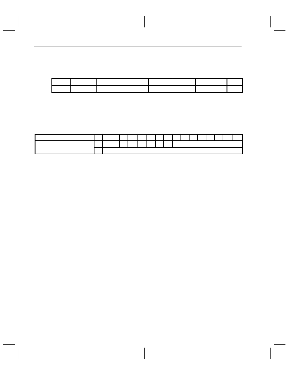
RTAG {adrs}
1
1
0
1
0
1
1
0
1
adrs
x
dma16 (for direct) or offset16 (long relative) [see section 4.13]
Description
Resets tag bit at addressed memory location. All addressing modes are
available. Note that this instruction accesses only the 17
th
bit of the RAM
location. For odd RAM byte addresses, the least significant bit is ignored.
See Also
STAG, RFLAG, SFLAG
Example 4.14.62.1
RTAG * 0x0200 * 2
Reset the tag bit of data memory word location to 0. Note that this operation can also be done with
RFLAG by loading the R6 register with * 0200 * 2.
Example 4.14.62.2
RTAG *R6+0x0002
Reset the tag bit of RAM location 0x0082. Assume R6 = 0x0080. Unlike the SFLAG and RFLAG
instructions, the argument of the STAG/RTAG instruction is interpreted as bytes.
Example 4.14.62.3
RTAG *R6+0x0003
Reset the tag bit of RAM location 0x0082. Assume R6 = 0x0080.
