7 rf detector d101, 8 power-control ic (pcic) u104, Rf detector d101 -14 – Motorola SSETM 5000 User Manual
Page 36: Power-control ic (pcic) u104 -14, Table 2-8, Power control ic (u104) pin descriptions -14
November 11, 2004
6881094C12-A
2-14
Theory of Operation: Transceiver Board
The initial design utilizes a cutoff frequency of 750 MHz, even though the actual design cutoff
frequency is 488 MHz. The reasoning behind using a significantly higher cutoff frequency is due to
the lower frequency response of realized circuits. The design tables used for the filter synthesis can
be located in the Handbook of Filter Synthesis (Zverev, pp. 218–219), where
θ
= 47.0. This design
was chosen because the attenuation at the stop band was the closest to the desired ratio for the
SSE 5000 design.
The remote port harmonic filter consists of parts C709, C710, C711, C712, C713, L706, and L707.
The antenna port harmonic filter consists of parts C716, C717, C718, C719, C720, L709, and L710.
The filters are optimized for the impedance match seen for their respective ports and terminations.
NOTE: Capacitor C720 was changed to 2pF, because this value improved the radiated response of
the radio with the antenna removed. Also, Capacitors C710 and C711 were increased in order
to remove a spur located at the (2*LO)-IF frequency point (680.075 MHz), where LO is
450.0625 MHz – 73.35 MHz and IF is 73.35 MHz. Essentially, C710 and C711 decreased the
cutoff frequency of the remote port harmonic filter.
2.4.3.7 RF Detector D101
Schottky diode D101 is used as a forward-power detector. Forward-coupled RF from the power
amplifier is converted to a DC voltage. Detector output is a positive DC voltage, proportional to the
amplitude of the RF signal at the input, and is applied to the ALC input of the PCIC.
2.4.3.8 Power-Control IC (PCIC) U104
The PCIC, U104, contains all of the digital, and most of the analog, circuits needed to control the
transmitter power amplifier. Host control is through a 3-wire, smart SPI interface. Pin descriptions are
shown in
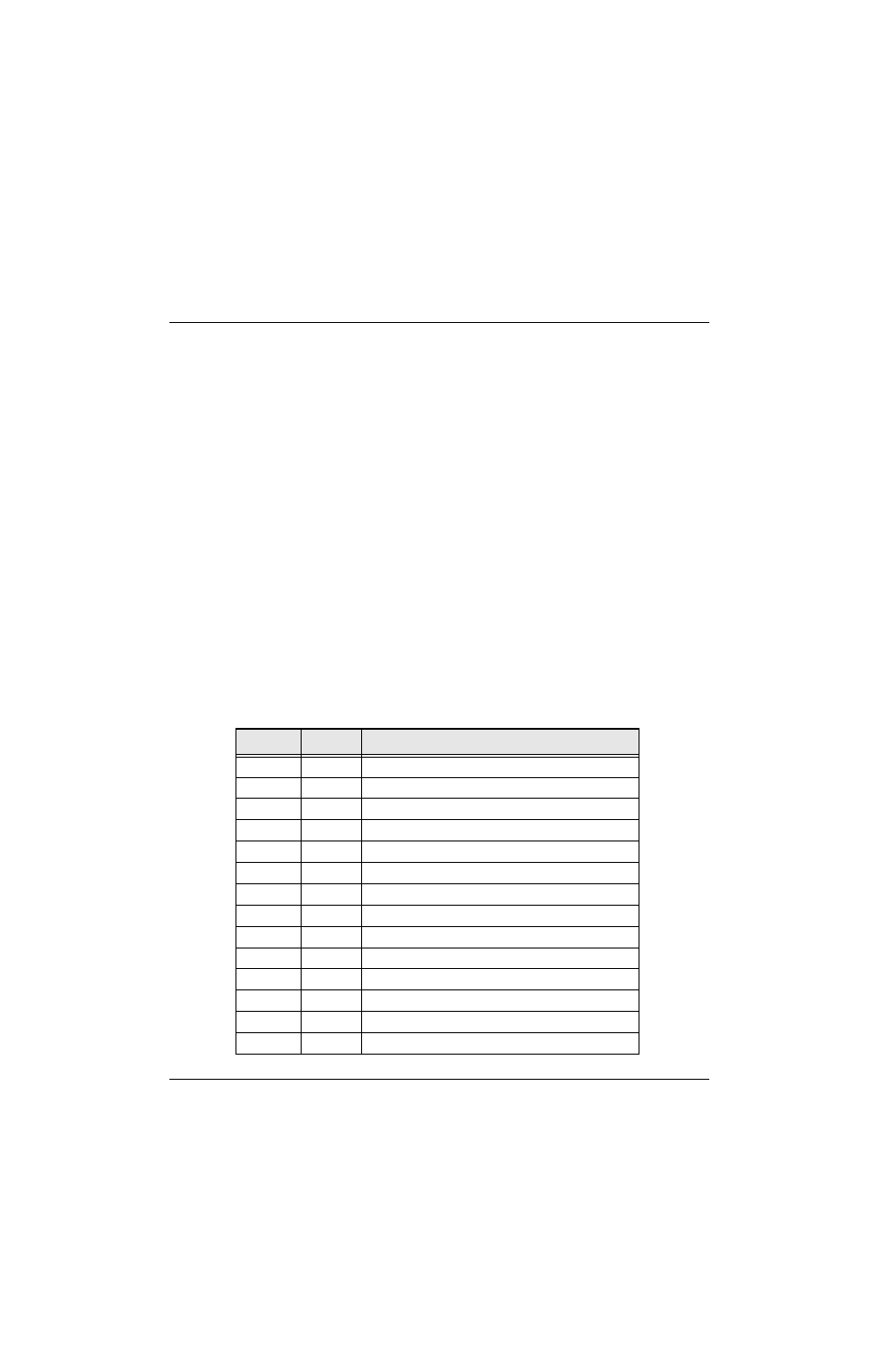
Table 2-8. Power Control IC (U104) Pin Descriptions
Pin
Name
Description
1
RFIN
Detector voltage input to ALC
2
T1
Test point
3
CI
External capacitor for integrator time constant
4
INT
Integrator output; control voltage to amplifiers
5
CJ
External capacitor for PA rise and fall times
6, 7
VL, CL
External capacitor for PA rise and fall times
8
GND1
Ground
9
F168
Reference clock input, 2.1 MHz
10, 13
QX, CQX
External capacitor for voltage multiplier
11, 12
Q, CQ
External capacitor for voltage multiplier
14
V10
Voltage multiplier output
15
VG
Internal band-gap reference voltage
16
V45
Regulated 4.5 Vdc output
17
V5EXT
Power supply input for internal voltage regulator