Vme connector pinout (p1 and p2), Figure a-2, Vme connector diagram (p1/p2) – FANUC Robotics America V7865* User Manual
Page 75
75
VME Connector Pinout (P1 and P2)
A
VME Connector Pinout (P1 and P2)
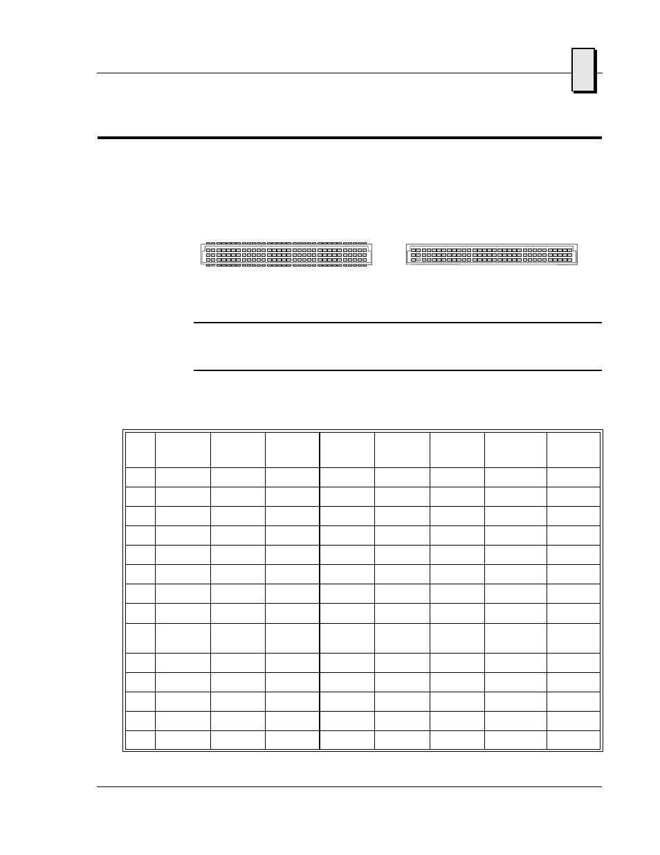
Figure A-2 and Table A-1 show the pin assignments for the VME connectors. Note
that only Row B of connector P2 is used; all other pins on P2 are reserved and should
not be connected.
Figure A-2 VME Connector Diagram (P1/P2)
WARNING
: The V7865 board should not be used with IDE rear cabling that is
compatible with any VME-74xx boards, except for the VME-7469, which supports
SATA.
Table A-1 VME Connector Pinout (P1/P2)
Pin#
P1 Row A
Signal
P1 Row B
Signal
P1 Row C
Signal
P2 Row Z
Signal
P2 Row A
Signal
P2 Row B
Signal
P2 Row C
Signal
P2 Row D
Signal
1
D00
BBSY#
D08
CONN [2]
GND
VCC_5.0
SP1_TX
CONN [1]
2
D01
BCLR#
D09
GND
USB_P5N
GND
SP1_RTS#
CONN [3]
3
D02
ACFAIL
D10
CONN [5]
USB_P5P
RETRY#
SP1_DTR#
CONN [4]
4
D03
BG0IN#
D11
GND
USB_OC5#
A24
SP1_RX
CONN [6]
5
D04
BG0OUT#
D12
CONN [8]
GND
A25
SP1_DCD#
CONN [7]
6
D05
BG1IN#
D13
GND
USB_P4N
A26
SP1_CTS#
CONN [9]
7
D06
BG1OUT#
D14
CONN [11]
USB_P4P
A27
SP1_DSR#
CONN [10]
8
D07
BG2IN#
D15
GND
USB_OC4#
A28
SP1_RI#
CONN [12]
9
GND
BG2OUT#
GND
CONN [14]
GND
A29
RTM_
SCONF_GP
CONN [13]
10
SYSCLK
BG3IN#
SYSFAIL#
GND
USB_P3P
A30
VCC_5.0
CONN [15]
11
GND
BG3OUT#
BERR#
CONN [17]
USB_P3N#
A31
VCC_-12 V
CONN [16]
12
DS1#
BR0#
SYSRST#
GND
USB_OC3#
GND
GND
CONN [18]
13
DS0#
BR1#
LWORD#
CONN [20]
GND
VCC_5.0
SATA1_RXN
CONN [19]
14
WRITE#
BR2#
AM5
GND
USB_P2N
D16
SATA1_RXP
CONN [21]
32
1
32
1
P2
P1
Row
D
C
B
A
Z