Timer control status register 2 (tcsr2) – FANUC Robotics America V7865* User Manual
Page 62
62
3
V7865 Product Manual
Each timer has an independently selectable clock source which is selected by the bit
pattern in the “Timer x Clock Select” field as follows:
Each timer can be independently enabled by writing a “1” to the appropriate “Timer x
Enable” field. Similarly, the generation of interrupts by each timer can be
independently enabled by writing a “1” to the appropriate “Timer x IRQ Enable”
field.
If an interrupt is generated by a timer, the source of the interrupt may be determined
by reading the “Timer x Caused IRQ” fields. If the field is set to “1”, then the
respective timer caused the interrupt. Note that multiple timers can cause a single
interrupt. Therefore, the status of all timers must be read to ensure that all interrupt
sources are recognized.
A particular timer interrupt can be cleared by writing a “0” to the appropriate “Timer
x Caused IRQ” field. Alternately, a write to the appropriate Timer x IRQ Clear (TxIC)
register will also clear the interrupt. When clearing the interrupt using the “Timer x
Caused IRQ” fields, note that it is very important to ensure that a proper bit mask is
used so that other register settings are not affected. The preferred method for clearing
interrupts is to use the “ Timer x IRQ Clear” registers described on page 65.
Timer Control Status Register 2 (TCSR2)
The timers are also controlled by bits in the Timer Control Status Register 2 (TCSR2)
located at offset 0x04 from the address in BAR2. The mapping of the bits in this
register are as follows:
The “Read Latch Select” bit is used to select the latching mode of the programmable
timers. If this bit is set to “0”, then each timer output is latched upon a read of any one
of its address. For example, a read to the TMRCCR12 register latches the count of
timers 1 and 2. A read to the TMRCCR3 register latches the count of timer 3. This
continues for every read to any one of these registers. As a result, it is not possible to
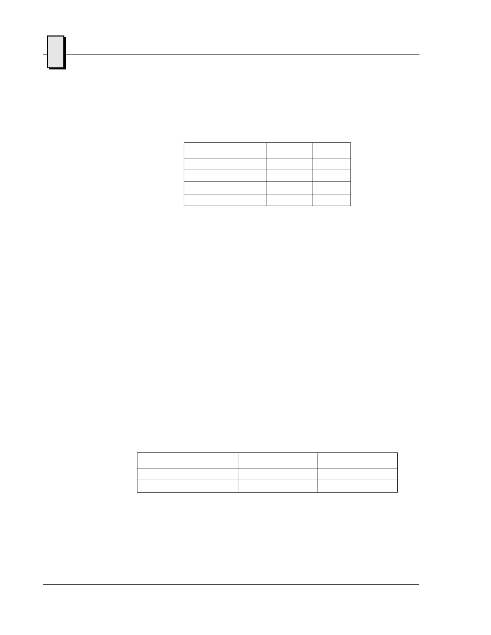
Clock Rate
MSb
LSb
2MHz
0
0
1MHz
0
1
500kHz
1
0
250kHz
1
1
Field
Bits
Read or Write
Read Latch Select
TCSR2[0]
Read/Write
Reserved
All Other Bits
Read/Write
All of these bits default to “0” after system reset.