Interlaken interface, Interlaken interface –40 – Altera 100G Development Kit, Stratix V GX Edition User Manual
Page 48
2–40
Chapter 2: Board Components
Components and Interfaces
100G Development Kit, Stratix V GX Edition
August 2012
Altera Corporation
Reference Manual
lists the CFP interface component reference and manufacturing
information.
Interlaken Interface
The Interlaken interface consists of 24 full-duplex transceiver channels with
AC-coupling on the receiver data. The header connector transmits data across the
interface while the receptacle connector receives data from the interface.
Since the pin labeling of the header and receptacle connectors are mirror image of
each other, the transmit and receive differential pairs have the same pin assignment.
For example, TX_P0 at A7 of header mates with RX_P0 at A7 of receptacle.
lists the pin assignments for the Interlaken interface and their
corresponding schematic signal names and Stratix V GX pin numbers.
132
CFP_TX_N6
1.5-V PCML
U3
Transmit XCVR pair 6 from FPGA
134
CFP_TX_P7
1.5-V PCML
R4
Transmit XCVR pair 7 from FPGA
135
CFP_TX_N7
1.5-V PCML
R3
Transmit XCVR pair 7 from FPGA
137
CFP_TX_P8
1.5-V PCML
N4
Transmit XCVR pair 8 from FPGA
138
CFP_TX_N8
1.5-V PCML
N3
Transmit XCVR pair 8 from FPGA
140
CFP_TX_P9
1.5-V PCML
J4
Transmit XCVR pair 9 from FPGA
141
CFP_TX_N9
1.5-V PCML
J3
Transmit XCVR pair 9 from FPGA
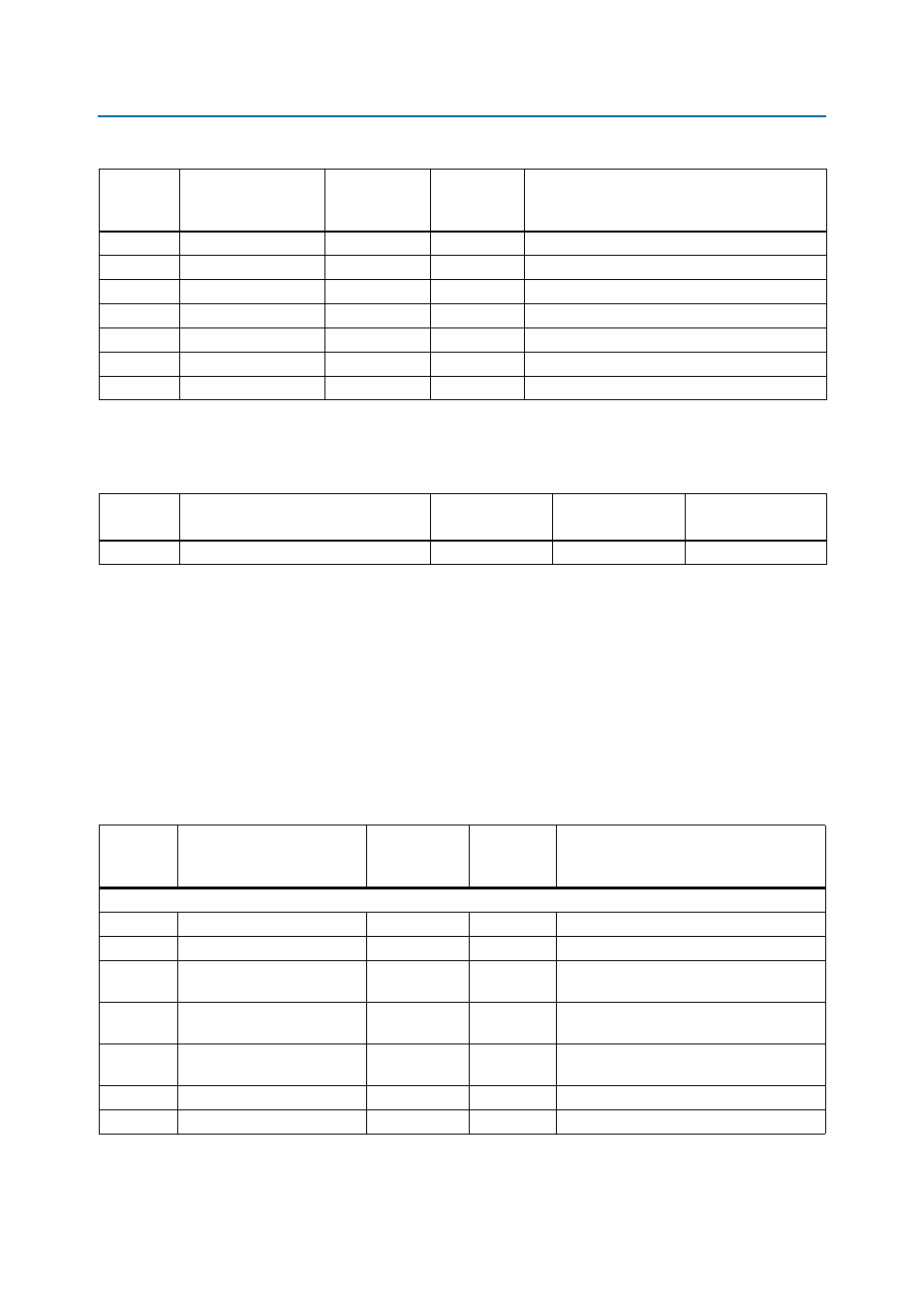
Table 2–31. CFP Interface Pin Assignments, Schematic Signal Names, and Functions (Part 4 of 4)
Board
Reference
(J25)
Schematic Signal
Name
I/O Standard
Stratix V GX
Device Pin
Number
Description
Table 2–32. CFP interface Component Reference And Manufacturing Information
Board
Reference
Description
Manufacturer
Manufacturing
Part Number
Manufacturer
Website
J25
CFP host board receptacle connector
Tyco Electronics
2057630-1
Table 2–33. Interlaken Interface Pin Assignments, Schematic Signal Names, and Functions (Part 1 of 5)
Board
Reference
Schematic Signal Name
I/O Standard
Stratix V GX
Device Pin
Number
Description
Interlaken Interface Channel 0-11 (J4, J16)
B1
INT_LSB_CON_TX_CLK_N
LVDS
—
Transmit clock for the first 12 bits of the bus
A1
INT_LSB_CON_TX_CLK_P
LVDS
—
Transmit clock for the first 12 bits of the bus
E10
INT_LSB_CON_TX_FC_CK
2.5-V LVCMOS
AM13
Transmit flow control clock signal for the
first 12 bits of the bus
H7
INT_LSB_CON_TX_FC_DATA
2.5-V LVCMOS
AR34
Transmit flow control data signal for the first
12 bits of the bus
H9
INT_LSB_CON_TX_FC_SYNC
2.5-V LVCMOS
AR32
Transmit flow control synchronization signal
for the first 12 bits of the bus
A7
INT_TX_P0
1.5-V PCML
AE41
Transmit XCVR pair 0 from FPGA
B7
INT_TX_N0
1.5-V PCML
AE42
Transmit XCVR pair 0 from FPGA