Pll settings tab, Receiver settings tab – Altera LVDS SERDES User Manual
Page 12
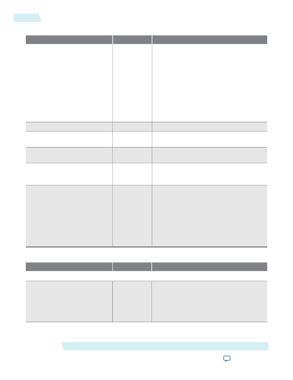
PLL Settings Tab
Description
Value
Parameter
When enabled, the IP core does not instantiate a
PLL locally. Instead, a series of clock connections
are elaborated with the prefix "ext" that should be
connected to an externally generated PLL. This
option allows you to access all of the available
clocks from the PLL, as well as use advanced PLL
features such as clock switchover, bandwidth
presets, dynamic phase stepping, and dynamic
reconfiguration.
The Clock Resource Summary tab guides you to
configure your external PLL.
—
Use external PLL
Specifies the
inclock
frequency in MHz
—
Desired inclock frequency
Specifies the closest
inclock
frequency to the
desired frequency that can source the interface.
—
Actual inclock frequency
Specifies the FPGA/PLL speed grade which
determines the operation range of the PLL.
—
FPGA/PLL speed grade
When enabled, this parameter exposes the
pll_
areset
port, which you can use to reset the entire
LVDS interface.
—
Enable pll_areset port
Specifies which clock network the Altera LVDS
SERDES IP core should export an internally
generated coreclock onto.
This feature is not supported in the
current version of the Quartus II
software. However, this can be
manually added using QSF
assignments.
Note:
—
Core clock resource type
Receiver Settings Tab
Description
Value
Parameter
Bitslip Settings
When enabled, this parameter adds a bitslip block
to the data path of the receiver and exposes the
rx_
bitslip_ctrl
port (one input per channel). Every
assertion of the
rx_bitslip_ctrl
signal adds one
bit of serial latency to the data path of the specified
channel.
—
Enable bitslip mode
Altera LVDS SERDES IP Core User Guide
Altera Corporation
ug_altera_lvds
PLL Settings Tab
12
2014.08.18