Digilent 410-138P-KIT User Manual
Page 9

Genesys Reference Manual
www.digilentinc.com
page 9 of 28
Copyright Digilent, Inc. All rights reserved. Other product and company names mentioned may be trademarks of their respective owners
Power
Jack
Battery
Connector
Power Select
Jumper JP13
VU
1.8V
1.0V
2.5V
3.3V
IC20
IC21
IC23
IC25
EN
Power
Switch
Vswt
IC24
EN
0.9V
.005
INA219
.005
INA219
.005
INA219
.005
INA219
To Digilent
Adept USB
I2C Bus
IC22
To Expansion
Connectors, LCD,
HDMI, USB
PG
PG
PG
PG
EN
EN
EN
Power On
LED (LD8)
TPS54620
6A Regulator
TPS54620
6A Regulator
TPS54620
6A Regulator
TPS54620
6A Regulator
ON
OFF
TPS51100
DDR Term. Reg.
Load Switch
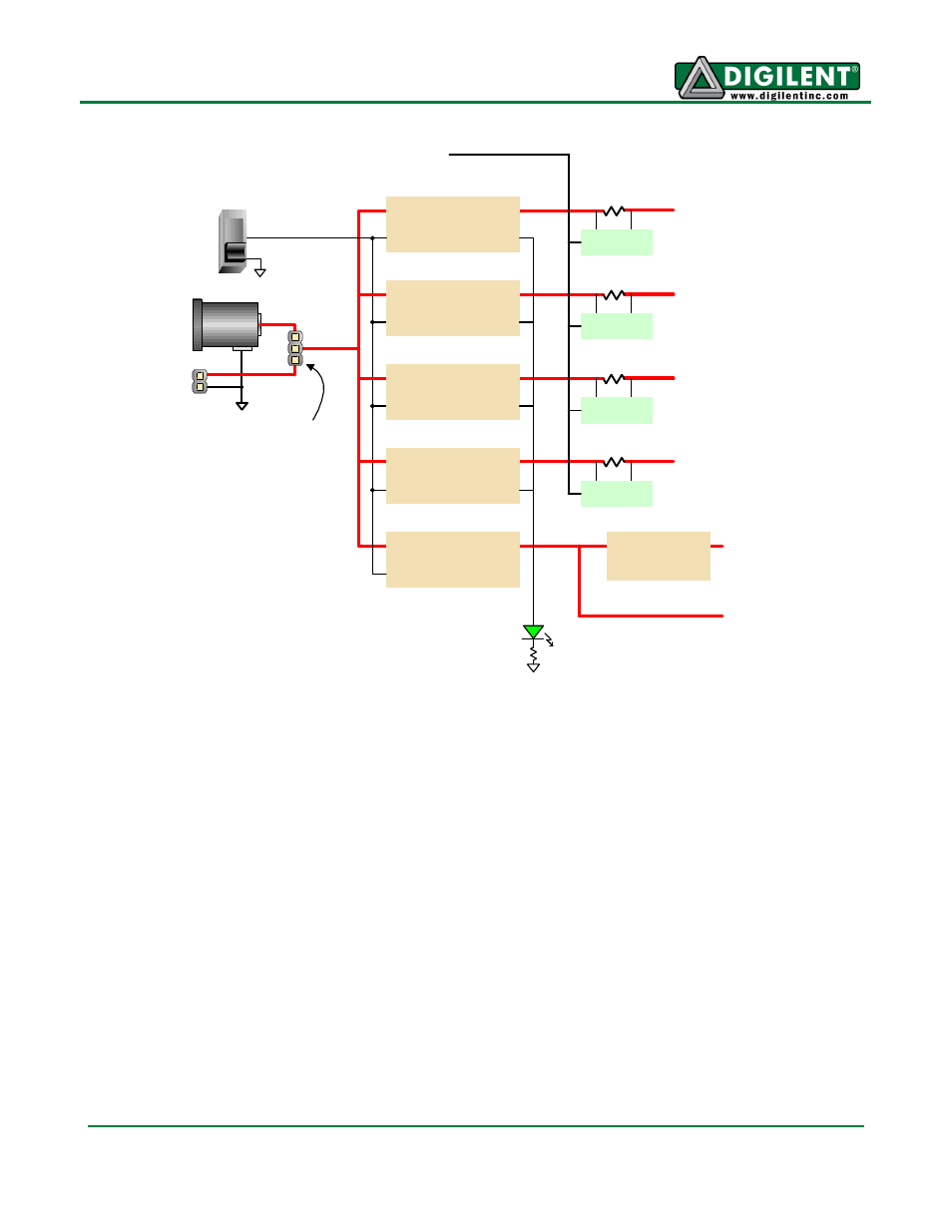
Genesys power supplies are controlled by a logic-level switch (SW9) that enables/disables the power
supply controller IC’s. A power-good LED (LD8), driven by the “power good” outputs on all supplies,
indicates that all supplies are operating within 10% of nominal.
A load switch (the TPS51100) passes the input voltage VU to the "Vswt" node, depending on the state
of the power switch. Vswt is assumed to be 5V, and is used by many systems on the board including
the LCD, HDMI ports, I2C bus, and USB host. Vswt is also available at expansion connectors, so that
any connected boards can be turned off along with the Genesys board.
DDR2 Memory
A single small outline dual in-line memory module (SODIMM) connector is provided and loaded with a
Micron MT4HTF3264HY-667D3 (or equivalent) single-rank unregistered 256Mbyte DDR2 module
(additional address lines and chip selects are routed, so that similar SODIMMs with densities up to
2GB may be used). Serial Presence Detect (SPD) using an IIC interface to the DDR DIMM is also
supported.
The Genesys board has been tested for DDR2 operation at a 400MHz data rate. Faster data rates
might be possible but are not tested.
