Digilent 410-138P-KIT User Manual
Page 19
Genesys Reference Manual
www.digilentinc.com
page 19 of 28
Copyright Digilent, Inc. All rights reserved. Other product and company names mentioned may be trademarks of their respective owners
Available instructions (and the
associated IR codes) are shown in the
right-most column of the “LCD
Instructions and Codes” table below. A
busy flag shows whether the display
has competed the last requested
operation; prior to initiating a new
operation, the flag can be checked to
see if the previous operation has been
completed.
The display has more DDRAM locations
than can be displayed at any given
time. DDRAM locations 00H to 27H
map to the first display row, and
locations 40H to 67H map to the second row. Normally, DDRAM location 00H maps to the upper left
display corner, and 40H to the lower left. Shifting the display left or right can change this mapping.
The display uses a temporary data register (DR) to hold data during DDRAM /CGRAM reads or
writes, and an internal address register to select the RAM location. Address register contents, set via
the IR, are automatically incremented after each read or write operation. RAM read/write requests will
be directed to DDRAM or CGRAM, depending on which address register was most recently accessed.
The LCD display uses ASCII character codes. Codes up through 7F are standard ASCII (which
includes all “normal” alphanumeric characters). Codes above 7F produce various international
characters – please see the Sitronix ST7066U data sheet for more information on international codes.
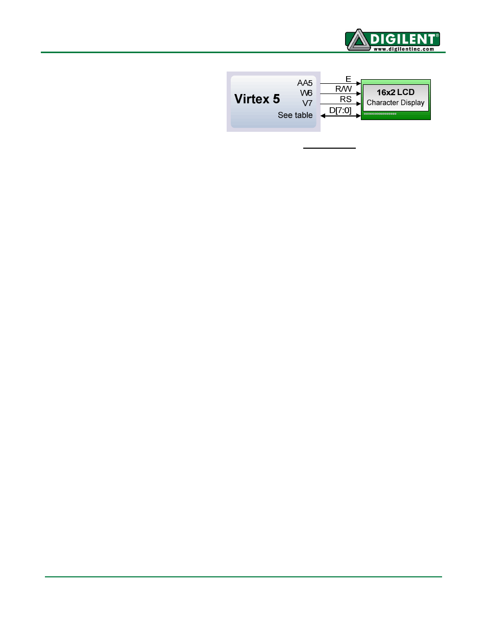
The display is connected to the Vitex FPGA by a 16-pin connector (pins 15 and 16 are for an optional
backlight, and they are not used). The 14-pin interface includes eight data signals, three control
signals, and three voltage supply signals. The eight bidirectional data bus signals communicate data
to the control registers or RAM locations. The RS (Register Strobe) signal clocks data into registers or
into RAM, the R/W signal determines bus direction, and the E signal enables the bus for read or write
operations. LCD bus signals and
timings are illustrated below.
A startup sequence with specific
timings ensures proper LCD
operation. After power-on, at least
20ms must elapse before the
function-set instruction code can
be written to set the bus width,
number of lines, and character
patterns (8-bit interface, 2 lines,
and 5x8 dots are appropriate).
After the function-set instruction,
at least 37us must elapse before
the display-control instruction can
be written (to turn the display on,
turn the cursor on or off, and set
the cursor to blink or no blink).
After another 37us, the display-
clear instruction can be issued.
LCD Signals
Signal LCD
Pin
FPGA
Pin
Signal Description
Vss
1
Ground
Vdd
2
5V Power Supply
Vo
3
Contrast Voltage (typically 100mV-200mV at 20C)
RS
4
V7
Register select: high for data, low for instructions
R/W
5
W6
Read/write signal: high for read, low for write
E
6
AA5
Read/write: high for OE; falling edge writes data
DB0
7
Y8
Bidirectional data bus 0
DB1
8
AB7
Bidirectional data bus 1
DB2
9
AB5
Bidirectional data bus 2
DB3
10
AC4
Bidirectional data bus 3
DB4
11
AB6
Bidirectional data bus 4
DB5
12
AC5
Bidirectional data bus 5
DB6
13
AC7
Bidirectional data bus 6
DB7
14
AD7
Bidirectional data bus 7
Data Signals
D0: Y8
D4: AB6
D1: AB7
D5: AC5
D2: AB5
D6: AC7
D3: AC4
D7: AD7