Usb host – Digilent 410-138P-KIT User Manual
Page 13
Genesys Reference Manual
www.digilentinc.com
page 13 of 28
Copyright Digilent, Inc. All rights reserved. Other product and company names mentioned may be trademarks of their respective owners
The Genesys BSB support package automatically generates a test application for the Ethernet MAC;
this can be used as a reference for creating custom designs. Another example Ethernet-based design
(the web server) can be found on the Digilent website.
ISE designs can use the IP Core Generator wizard to create a tri-mode Ethernet MAC controller IP
core.
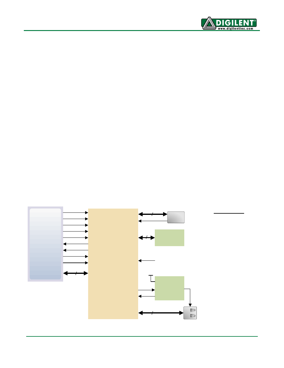
USB Host
A Cypress CY7C67300 USB controller provides the Genesys board with USB host and peripheral
capability. The CY7C67300 includes two serial interface engines (SIE) that can be used
independently. SIE1 is connected to a Type A USB host connector (J8), and SIE2 is connected to a
Type B USB peripheral connector (J9).
The USB controller has an internal microprocessor to assist in processing USB commands; a
dedicated IIC EEPROM (IC9) is available for storing firmware. Firmware can be developed for the
processor and/or written to the EEPROM using the Cypress CY3663 EZ-OTG™/EZ-Host™
development kit available from Cypress.
To assist with debug, the USB controller's two-wire serial port is connected to two FPGA pins (USB-
RX to FPGA pin V9, USB-TX to FPGA pin W7) using LVCMOS33 I/O standards. Jumper JP14 can be
installed to prevent the USB controller from executing firmware stored in the IIC EEPROM.
To access the USB host controller, EDK designs can use the xps_epc IP core. Reference designs
posted on the Digilent website show an example for reading characters from a USB keyboard
connected to the USB host interface.
See Table
V9
AF6
AE6
AD4
Virtex 5
AE7
AD5
CS
WR
RD
INT
TX
A0
2
A1
AD6
D[15:0]
16
Cypress CY7C67300
USB Host
Type A
USB Periph
Type B
2
I2C ROM
TPS2041
24AA128
Vswt
HOST_EN
2
I2C
12MHz
(from IDT5V9885)
CLK
RX
W7
RESET
AJ6
Over_Current
USB Power
Switch
EN
OC#
V_INT
Vusbp
Vusbh
Data Signals
D0: Y6
D1: AA6
D2: Y7
D3: Y9
D4: W10
D5: AC5
D6: Y11
D7: AJ7
D8: AH7
D9: AH5
D10: AG6
D11: AG7
D12: AK7
D13: AK6
D14: AG5
D15: AF5