Virtex 5 ddr2 sodimm – Digilent 410-138P-KIT User Manual
Page 10
Genesys Reference Manual
www.digilentinc.com
page 10 of 28
Copyright Digilent, Inc. All rights reserved. Other product and company names mentioned may be trademarks of their respective owners
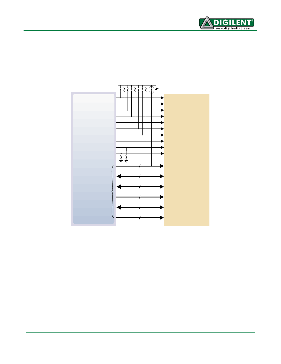
The DDR2 interface follows the pinout and routing guidelines specified in the Xilinx Memory Interface
Generator (MIG) User Guide. The interface supports SSTL18 signaling, and all address, data, clocks,
and control signals are delay-matched and impedance-controlled. Address and control signals are
terminated through 47-ohm resistors to a 0.9V V
TT
, and data signals use the On-Die-Termination
(ODT) feature of the SODIMM. Two well-matched DDR2 clock signal pairs are provided to the
SODIMM that can be driven with low-skew clocks from the FPGA.
DQ[63:0]
DS[7:0] (differential)
14
64
16
AD[13:0]
I2C (SDA, SCK)
8
RAS#
CAS#
WE#
BA0
BA1
BA2
Clocks (differential)
6
S0#
S1#
ODT0
See Table
ODT1
F30
F31
J29
L29
R31
J30
G31
K29
E31
H30
Virtex 5
DDR2
SODIMM
DM[7:0]
2
x14
- 410-282P-KIT (4 pages)
- 410-279P-KIT (26 pages)
- 410-258P-KIT (16 pages)
- 410-178P-KIT (22 pages)
- 410-292P-KIT (29 pages)
- 410-274P-KIT (29 pages)
- 410-182P-KIT (22 pages)
- 410-134P-KIT (17 pages)
- 410-183P-KIT (19 pages)
- 410-155P-KIT (12 pages)
- 6015-410-001P-KIT (26 pages)
- 410-087P-KIT (164 pages)
- 410-146P-KIT (4 pages)
- 6003-410-000P-KIT (138 pages)
- XUPV2P (23 pages)
- 410-047-C2P-KIT (3 pages)
- WaveForms (85 pages)
- 410-297P-KIT (25 pages)
- 410-295P-KIT (37 pages)
- 410-296P-KIT (23 pages)
- 410-209P-KIT REV.D (16 pages)
- 410-209P-KIT REV.C (17 pages)
- 410-254P-KIT (17 pages)
- 410-280P-KIT (9 pages)
- 410-202P-KIT (20 pages)
- 410-273P-KIT (24 pages)
- 410-269P-KIT (11 pages)
- 410-216P-KIT (15 pages)
- 410-231P-KIT (4 pages)
- 410-211P-KIT (10 pages)
- 410-262P-KIT (8 pages)
- 410-229P (7 pages)
- 410-242P-KIT (4 pages)
- 6021-210-000P-KIT (27 pages)
- 410-185P-KIT (21 pages)
- 6032-410-000P-BOARD (4 pages)
- 410-174P (17 pages)
- 410-145P (6 pages)
- 210-264P-BOARD (3 pages)
- 6003-210-012P (27 pages)
- 410-236P-BOARD (2 pages)
- 410-163P (1 page)
- 410-097P-KIT (2 pages)
- 410-255P-KIT (1 page)