Built-in self test – Digilent 410-138P-KIT User Manual
Page 28
Genesys Reference Manual
www.digilentinc.com
page 28 of 28
Copyright Digilent, Inc. All rights reserved. Other product and company names mentioned may be trademarks of their respective owners
a user-defined selection of parameters to be automatically monitored, and user-programmable
averaging is enabled to ensure robust noise-free measurements.
The System Monitor also provides user-programmable alarm thresholds for the on-chip sensors.
Thus, if an on-chip monitored parameter moves outside the user-specified operating range, an alarm
logic output becomes active. In addition to monitoring the on-chip temperature for user-defined
applications, the System Monitor issues a special alarm called Over-Temperature (OT) if the FPGA
temperature becomes critical (> 125°C). The OT signal is deactivated when the device temperature
falls below a user specified lower limit. If the FPGA power-down feature is enabled, the FPGA enters
power down when the OT signal becomes active. The FPGA powers up again when the alarm is
deactivated. For additional information about the System Monitor, see
http://www.xilinx.com/systemmonitor
and consult the Virtex 5 FPGA System Monitor User Guide. The
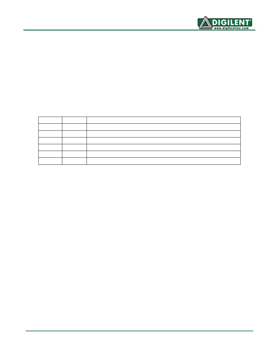
table below shows the System Monitor connections.
Built-In Self Test
A demonstration configuration is loaded into the StataFlash ROM on the Genesys board during
manufacturing. This demo, also available on the Digilent website, can serve as a board verification
test since it interacts with all devices and ports on the board. To configure the FPGA from the demo
file stored in StrataFlash, set the mode jumper to BPI UP and cycle power. When Genesys powers
up, the DDR is tested, and then an image file will be transferred from the StrataFlash into DDR2. This
image will be driven out the HDMI port for display on a DVI/HDMI compatible monitor. The slide
switches are connected to the user LEDs, and user buttons BTN0, BTN1, and BTN3 cause varying
sine-wave frequencies to be driven on the LINE IN and LINE OUT audio ports. The LCD screen
(DISP1) will initially display “Genesys User Demo / BIST” on startup, and then display text whenever
the state of a user button or switch is changed.
If the self test is not resident in the StrataFlash ROM, it can be programmed into the FPGA or
reloaded into the ROM using the Adept programming software.
All Genesys boards are 100% tested during the manufacturing process. If any device on the Genesys
board fails test or is not responding properly, it is likely that damage occurred during transport or
during use. Typical damage includes stressed solder joints and contaminants in switches and buttons
resulting in intermittent failures. Stressed solder joints can be repaired by reheating and reflowing
solder, and contaminants can be cleaned with off-the-shelf electronics cleaning products. If a board
fails test within the warranty period, it will be replaced at no cost. If a board fails test outside of the
warranty period and cannot be easily repaired, Digilent can repair the board or offer a discounted
replacement. Contact Digilent for more details.
J13 Pin
Signal
Function
1
DXP
Anode of the FPGA temperature-sensing diode
2
VP
System Monitor dedicated differential analog input (positive side)
3
DXN
Cathode of the FPGA temperature-sensing diode
4
VN
System Monitor dedicated differential analog input (negative side)
5
GND
6
GND