Digilent 410-138P-KIT User Manual
Page 7
Genesys Reference Manual
www.digilentinc.com
page 7 of 28
Copyright Digilent, Inc. All rights reserved. Other product and company names mentioned may be trademarks of their respective owners
supplies for up to ten minutes. Recorded values
are also stored in a buffer that can be saved to a
file for later analysis. Save Buffer and Clear
Buffer are used to save and clear the historical
data in the buffer.
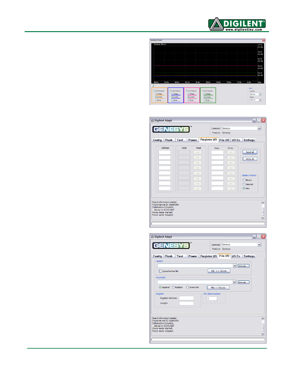
Register I/O
The register I/O tab requires that a corresponding
IP block, available in the Parallel Interface
reference design (DpimRef.vhd) on the Adept
page of the Digilent website, is included and
active in the FPGA. This IP block provides an
EPP-style interface, where an 8-bit address
selects a register, and data read and write
buttons transfer data to and from the selected
address. Addresses entered into the address field
must match the physical address included in the
FPGA IP block.
Register I/O provides an easy way to move small
amounts of data into and out of specific registers
in a given design. This feature greatly simplifies
passing control parameters into a design, or
reading low-frequency status information out of a
design.
File I/O
The File I/O tab can transfer arbitrarily large files
between the PC and the Genesys FPGA. A
number of bytes (specified by the Length value)
can be streamed into a specified register address
from a file or out of a specified register address
into a file. During upload and download, the file
start location can be specified in terms of bytes.
As with the Register I/O tab, File I/O also requires
specific IP to be available in the FPGA. This IP
can include a memory controller for writing files
into the on-board DDR2 and Flash memories.