Expansion connectors – Digilent 410-138P-KIT User Manual
Page 25
Genesys Reference Manual
www.digilentinc.com
page 25 of 28
Copyright Digilent, Inc. All rights reserved. Other product and company names mentioned may be trademarks of their respective owners
Expansion Connectors
The Genesys board offers two 68-pin VHDC connectors for high-speed parallel I/O, and four 8-pin
Pmod connectors for lower speed and lower pin-count I/O. Data sheets for VHDC connectors can be
found on the Digilent website and on many vendor and distributor websites as well.
The VHDC connectors include 40 data signals (routed as 20 impedance-controlled matched pairs), 20
grounds (one per pair), and eight power signals. These connectors, commonly used for SCSI-3
applications, can accommodate data rates of several hundred megahertz on every pin. Both board-to-
board and board-to-cable mating connectors are available. Digilent and several distributors carry
mating connectors and cables of various lengths.
External circuits connected the VHDC expansion connectors can receive 2.5V or 3.3V supplies from
Genesys, depending on the position of power supply selection jumpers. Jumper JP11 selects the
voltage provided to VHDC connector J1 and the associated FPGA I/O bank 11, and jumper JP12
selects the supply for VHDC connector J2 and FPGA I/O bank 12 (all I/O’s to the connectors are
routed as matched pairs to support LVDS signaling). The VHDC connectors also include two pins
connected directly to in the input voltage VSWT; jumper JP1 can break that connection if required.
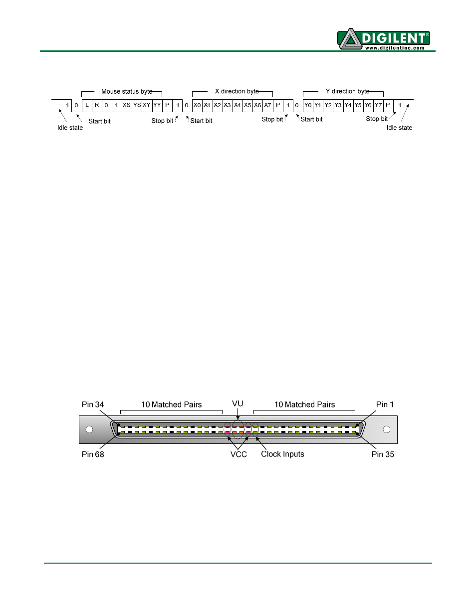
The VHDC connectors, labeled J1 and J2 on the first page of the schematic, use symmetrical pinouts
(as reflected around the vertical axis of the physical connector) so that peripheral boards as well as
other system boards can be connected. Connector pins 15 and 49 are routed to FPGA clock input
pins.
The Genesys board’s unregulated input voltage (VU) is routed to the four center pins of the connector,
providing up to 1A of current (250mA per pin) to connected boards. VU is routed to the connectors
through the main power switch, and through jumper JP1 (so that VU can be removed from peripheral
boards if desired).
All I/O pins on connector J1 are routed to FPGA I/O bank 11, and all I/O pins on connector J2 are
routed to FPGA I/O bank 13. The VCC voltage driving these I/O banks is also routed to four VCC pins
on each connector, using pins immediately distal to the four VU pins. The shared I/O bank and
Mouse Data Format