4 data memory write – Cypress Perform CY7C68013 User Manual
Page 40
CY7C68013A, CY7C68014A
CY7C68015A, CY7C68016A
Document #: 38-08032 Rev. *L
Page 40 of 62
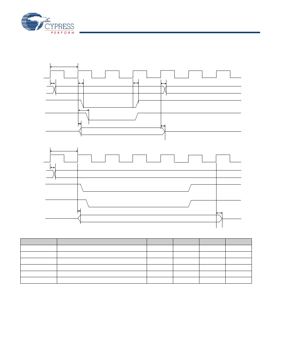
10.4 Data Memory Write
Figure 14. Data Memory Write Timing Diagram
When using the AUTPOPTR1 or AUTOPTR2 to address external memory, the address of AUTOPTR1 is only active while either RD#
or WR# are active. The address of AUTOPTR2 is active throughout the cycle and meets the above address valid time for which is
based on the stretch value.
t
OFF1
CLKOUT
A[15..0]
WR#
t
AV
D[7..0]
t
CL
t
STBL
t
STBH
data out
t
OFF1
CLKOUT
A[15..0]
WR#
t
AV
D[7..0]
t
CL
data out
Stretch = 1
t
ON1
t
SCSL
t
AV
CS#
t
ON1
CS#
Table 17. Data Memory Write Parameters
Parameter
Description
Min
Max
Unit
Notes
t
AV
Delay from Clock to Valid Address
0
10.7
ns
t
STBL
Clock to WR Pulse LOW
0
11.2
ns
t
STBH
Clock to WR Pulse HIGH
0
11.2
ns
t
SCSL
Clock to CS Pulse LOW
13.0
ns
t
ON1
Clock to Data Turn-on
0
13.1
ns
t
OFF1
Clock to Data Hold Time
0
13.1
ns
- CY7C1410AV18 (29 pages)
- CY7C1411JV18 (28 pages)
- CY7C1383FV25 (28 pages)
- CY14B256L (18 pages)
- CY7C1307BV25 (21 pages)
- CY7C1041DV33 (13 pages)
- CY62167EV18 (13 pages)
- Perform CY7C1565V18 (28 pages)
- STK11C68-5 (15 pages)
- 7C185-20 (11 pages)
- CY7C1168V18 (27 pages)
- CY7C1318CV18-250BZC (26 pages)
- CY7C1364C (18 pages)
- Perform CY7C1382D (34 pages)
- CY7C106D (11 pages)
- CY14E102N (21 pages)
- CY7C1418AV18 (31 pages)
- enCoRe CY7C638xx (83 pages)
- CY7C1018DV33 (9 pages)
- CY7C1292DV18 (23 pages)
- CY7C130 (19 pages)
- CY7C1424BV18 (30 pages)
- CY62157EV18 (12 pages)
- CY7C1392BV18 (31 pages)
- CY7C1302DV25 (18 pages)
- Perform CY7C1511KV18 (31 pages)
- West Bridge Astoria AN46860 (4 pages)
- CY7C1386FV25 (30 pages)
- CY7C1163V18 (29 pages)
- CY7C1266V18 (27 pages)
- CY7C1334H (13 pages)
- CY7C1018CV33 (7 pages)
- CY62136VN (12 pages)
- AN20639 (3 pages)
- CY7C1338G (17 pages)
- CY7C1462AV33 (27 pages)
- CY7C1145V18 (28 pages)
- STK11C88 (15 pages)
- CY7C1231H (12 pages)
- Perform CY7C142 (15 pages)
- CY14E256L (18 pages)
- STK15C88 (15 pages)
- CY7C1297H (15 pages)
- CY7C1441AV33 (31 pages)
- CapSense CY8C20x36 (34 pages)