2 program memory read – Cypress Perform CY7C68013 User Manual
Page 38
CY7C68013A, CY7C68014A
CY7C68015A, CY7C68016A
Document #: 38-08032 Rev. *L
Page 38 of 62
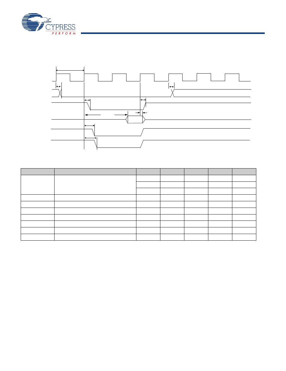
10.2 Program Memory Read
Figure 12. Program Memory Read Timing Diagram
t
CL
t
DH
t
SOEL
t
SCSL
PSEN#
D[7..0]
OE#
A[15..0]
CS#
t
STBL
data in
t
ACC1
t
AV
t
STBH
t
AV
CLKOUT
Table 15. Program Memory Read Parameters
Parameter
Description
Min
Typ
Max
Unit
Notes
t
CL
1/CLKOUT Frequency
20.83
ns
48 MHz
41.66
ns
24 MHz
83.2
ns
12 MHz
t
AV
Delay from Clock to Valid Address
0
10.7
ns
t
STBL
Clock to PSEN Low
0
8
ns
t
STBH
Clock to PSEN High
0
8
ns
t
SOEL
Clock to OE Low
11.1
ns
t
SCSL
Clock to CS Low
13
ns
t
DSU
Data Setup to Clock
9.6
ns
t
DH
Data Hold Time
0
ns
Notes
17. CLKOUT is shown with positive polarity.
18. t
ACC1
is computed from the above parameters as follows:
t
ACC1
(24 MHz) = 3*t
CL
– t
AV
– t
DSU
= 106 ns
t
ACC1
(48 MHz) = 3*t
CL
– t
AV
– t
DSU
= 43 ns.
- CY7C1410AV18 (29 pages)
- CY7C1411JV18 (28 pages)
- CY7C1383FV25 (28 pages)
- CY14B256L (18 pages)
- CY7C1307BV25 (21 pages)
- CY7C1041DV33 (13 pages)
- CY62167EV18 (13 pages)
- Perform CY7C1565V18 (28 pages)
- STK11C68-5 (15 pages)
- 7C185-20 (11 pages)
- CY7C1168V18 (27 pages)
- CY7C1318CV18-250BZC (26 pages)
- CY7C1364C (18 pages)
- Perform CY7C1382D (34 pages)
- CY7C106D (11 pages)
- CY14E102N (21 pages)
- CY7C1418AV18 (31 pages)
- enCoRe CY7C638xx (83 pages)
- CY7C1018DV33 (9 pages)
- CY7C1292DV18 (23 pages)
- CY7C130 (19 pages)
- CY7C1424BV18 (30 pages)
- CY62157EV18 (12 pages)
- CY7C1392BV18 (31 pages)
- CY7C1302DV25 (18 pages)
- Perform CY7C1511KV18 (31 pages)
- West Bridge Astoria AN46860 (4 pages)
- CY7C1386FV25 (30 pages)
- CY7C1163V18 (29 pages)
- CY7C1266V18 (27 pages)
- CY7C1334H (13 pages)
- CY7C1018CV33 (7 pages)
- CY62136VN (12 pages)
- AN20639 (3 pages)
- CY7C1338G (17 pages)
- CY7C1462AV33 (27 pages)
- CY7C1145V18 (28 pages)
- STK11C88 (15 pages)
- CY7C1231H (12 pages)
- Perform CY7C142 (15 pages)
- CY14E256L (18 pages)
- STK15C88 (15 pages)
- CY7C1297H (15 pages)
- CY7C1441AV33 (31 pages)
- CapSense CY8C20x36 (34 pages)