Programming overview, Understand module memory organization, Chapter 4 – Rockwell Automation 1746-BAS-T SLC 500 Basic Basic-T Modules User Manual
Page 49: Understand module memory organization -1, Chapter
1
Publication 1746-UM004B-EN-P - December 2005
Chapter
4
Programming Overview
This chapter provides an overview of the information needed to
program your module. After reading this chapter, you should be
familiar with:
• module memory organization.
• SLC memory allocation for your module.
• BASIC programming instructions.
• entering, running, and editing a BASIC program from an ASCII
terminal.
• interfacing the module with other devices.
Understand Module
Memory Organization
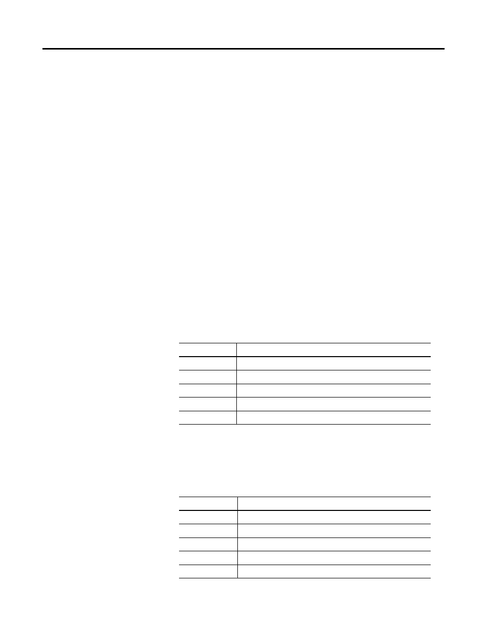
All data transferred to the module from the SLC 500 CPU must be
routed through the module input buffer. The following table lists the
addresses of the module input buffer.
All data transferred from the module to the SLC 500 CPU must be
routed through the module output buffer. The following table lists the
addresses of the module output buffer.
Address
Definition
0...39
Data transferred from the DH485 common interface file.
40...99
Reserved
100...163
Data transferred from the CPU M0 file.
164...199
Reserved
200...207
Data transferred from the CPU output image table.
Address
Definition
0...39
Data transferred to the DH485 common interface file.
40...99
Reserved
100...163
Data transferred to the CPU M1 file.
164...199
Reserved
200...207
Data transferred to the CPU input image table.