Rockwell Automation 1771-OFE/B Analog Output Module User Manual User Manual
Page 43
4-7
Publication 1771Ć6.5.30 - November 1998
Figure 4.4
PLCĆ3 Sample Program Structure
BLOCK XFER WRITE
Rack Addrress:
Group Address:
Module Address:
Data Address:
xxx
x
xxxxxx
xxxxx:xxxx
Length:
CNTL:
x
xxxxx:xxxx
U
Read Block Transfer Done Bit
Storage Bit
L
Write Block Transfer Done Bit
Storage Bit
FILES FROM A TO R
File A:
File R:
Counter Address:
Position/Length:
xxxxx:xxxx
xxxxx:xxxx
xxxxx
0/x
EN
Mode:
All/Scan
Read Block Transfer Done Bit
Enable
12
DN
Done
15
Storage Bit
ER
Error
BLOCK XFER READ
Rack Address:
Group Address:
Module Address:
Data Address:
xxx
x
xxxxxx
xxxxx:xxxx
Length:
CNTL:
x
xxxxx:xxxx
EN
Enable
12
DN
Done
15
ER
Error
13
Storage Bit
EN
Enable
02
DN
Done
05
ER
Error
03
1
2
3
4
5
BTW
BTR
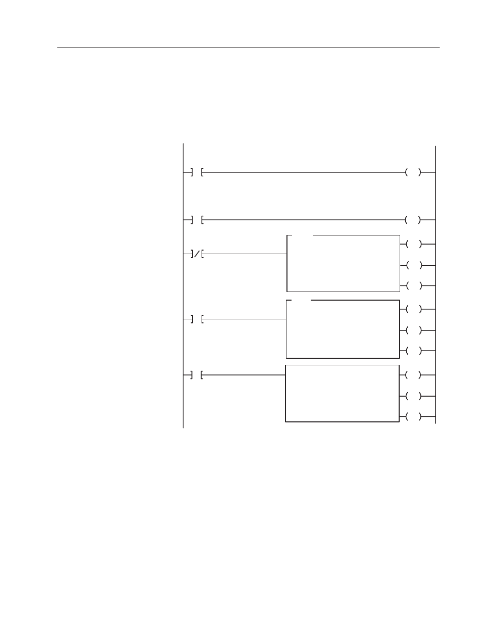
Rungs 1 and 2
The first two rungs of the sample
program segment toggle requests for
the read and write instructions. Notice
that the EXAMINE ON instructions in
Rungs 1 and 2 are the done bits of the
read and write instructions. By latching
or unlatching a storage bit, the write
done bit (XXXXX:XXXX/05) triggers the
BTR instruction and the read done bit
(XXXXX:XXXX/15) triggers the BTW
instruction.
Rung 3
The write block transfer instruction in
Rung 3 sends configuration, output, and
scaling data to the module from the
processor in one program scan.
Rung 4
The read block transfer instruction in
Rung 4 sends module status
information and a copy of the output
data to the processor from the module
in one program scan.
Rung 5
When a read block transfer has been
successfully completed, its done bit is set.
When the done bit (XXXXX:XXXX/15) is
set, it enables the fileĆtoĆfile move
instruction. The read block transfer data
file (buffer) is then moved into a storage
data file. This prevents the processor
from transmitting invalid data should a
block transfer communication fault occur.
At powerĆup, the program performs a write block transfer that configures the module. When the first write block transfer is complete, the
program toggles between read and write block transfers. The program takes into account that the read and write request bits cannot be set
simultaneously.
Upon completion of a successful read block transfer, data from the module is moved from the buffer file (block transfer read file) to a storage
data file. This prevents the module from using invalid data should block transfer communications fail.
Program Action