Rockwell Automation 1771-OFE/B Analog Output Module User Manual User Manual
Page 38
4-2
Publication 1771Ć6.5.30 - November 1998
Output data is transferred from the processor’s data table to the
module with a write block transfer. Diagnostic information is
transferred from the module to the processor’s data table with a read
block transfer. In order for these transfers to take place, you must
enter certain parameters into your block transfer instructions. A
sample program segment with block transfer read and write is shown
in Figure 4.1 and described in the following paragraphs.
An example program with block transfer instructions is shown in
Figure 4.2. A data table map (Table 4.A) and a data table word
assignment (Table 4.B) are also shown. Figure 4.3 shows how the
binary representation of configuration options is represented in BCD
(as it appears in our data table map).
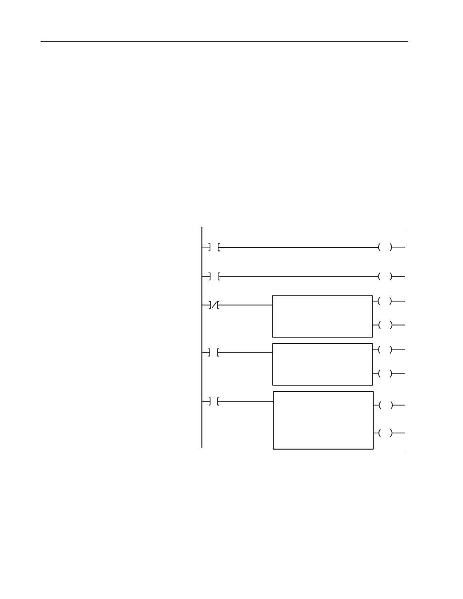
Figure 4.1
PLCĆ2 Family Sample Program Structure
U
Read Block Transfer Done Bit
Storage Bit
L
Write Block Transfer Done Bit
Storage Bit
BLOCK XFER WRITE
Data Address:
Module Address:
Block Length:
File:
xxx
RGS
00
xxx-xxx
EN
Storage Bit
Enable
16
DN
Done
16
FILE TO FILE MOVE
Counter Address:
Position:
File Length:
File A:
xxx
xxx
xxx
xxx-xxx
EN
File R:
Rate per Scan:
xxx-xxx
xxx
Read Block Transfer Done Bit
Enable
17
DN
Done
15
BLOCK XFER READ
Data Address:
Module Address:
Block Length:
File:
xxx
RGS
00
xxx-xxx
EN
Storage Bit
Enable
17
DN
Done
17
1
2
3
4
5
Program Action
Rungs 1 and 2
The first two rungs of the sample program segment
toggle requests for the read and write instructions.
Notice that the EXAMINE ON instructions in Rungs 1
and 2 are the done bits of the read and write
instructions. By latching or unlatching a storage bit,
the write done bit (XXX/X6) triggers the read block
transfer instruction and the read done bit (XXX/X7)
triggers the write block transfer instruction.
The write block transfer instruction in Rung 3 sends
configuration, output, and scaling data to the module
from the processor in one program scan.
The read block transfer instruction in Rung 4 sends
module status information and a copy of the output data
to the processor from the module in one program scan.
When a read block transfer has been successfully
completed, its done bit (Bit XXX/X7) is set. When the
done bit is set, it enables the fileĆtoĆfile move instruction.
The read block transfer data file (buffer) is then moved
into a storage data file. This prevents the processor from
transmitting invalid data should a block transfer
communication fault occur.
Rung 5
Rung 4
Rung 3
Upon completion of a successful read block transfer,
data from the module is moved from the buffer file
(block transfer read file) to a storage data file. This
prevents the processor from using invalid data should
block transfer communications fail.
At powerĆup, the program performs a write block
transfer that configures the module. When the first
write block transfer is complete, the program toggles
between read and write block transfers. The program
takes into account that the read and write request bits
cannot be set simultaneously.
Block Transfer
Programming Ć PLCĆ2
Family Processors Only