2 configuration options, 1 s/pdif in to s/pdif and pcm out, Figure 2.s/pdif in to s/pdif and pcm out – Cirrus Logic CDB8422 User Manual
Page 7: Section 2.2, Cdb8422
DS692DB2
7
CDB8422
2.2
Configuration Options
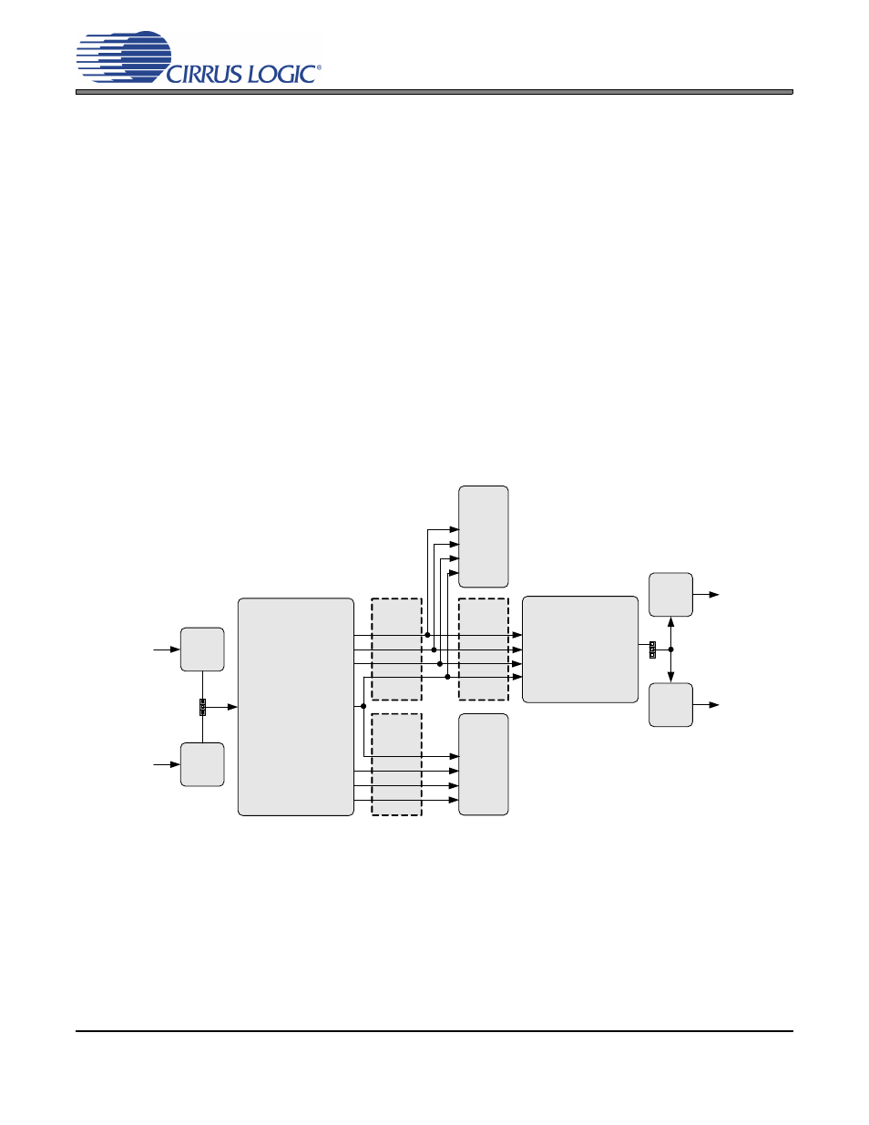
In software mode, to configure the CDB8422 for making performance measurements, one needs to use Cir-
rus Logic’s Windows compatible FlexGUI software to program the various components on the board. This
section serves to give a deeper understanding of the on-board circuitry and the digital clock and data signal
routing involved in several common software mode configurations of the CDB8422. These scripts only serve
as a starting point; after loading a script, the GUI can be further configured as needed (clock ratios, serial
formats, etc).
2.2.1
S/PDIF In to S/PDIF and PCM Out
The CS8422’s S/PDIF receiver and SRC output performance can be tested by loading the “SPDIF In to
SPDIF and PCM Out” quick setup file provided with the software package. The script configures the dig-
ital clock and data signal routing on the board as shown in
Digital S/PDIF input can be provided on the optical (J1) or RCA (J7) jacks. Jumper J4 selects which input
signal is connected to the RX0 pin of the CS8422. The script configures the CS8422’s internal circuitry to
send the input audio data through its SRC to serial output port 1. This data is presented as PCM audio at
header J24 and S/PDIF audio at J27 (coaxial) and J28 (optical). The input data is also passed through
(SRC is bypassed) to serial output port 2. This data is presented as PCM audio at header J25. Refer to
for details on software configuration.
Figure 2.
S/PDIF In to S/PDIF and PCM Out
CS8422
CS8406
S/PDIF Tx
Optical
S/PDIF In
(SLAVE)
J1
OR
RX0
Buffer
Buffer
Header
J24
Buffer
Header
J25
(MASTER)
(MASTER)
J7
J4
Coaxial
S/PDIF In
OSCLK1
OLRCK1
SDOUT1
OSCLK2
OLRCK2
SDOUT2
ISCLK
ILRCK
SDIN
OSCLK2
OLRCK2
SDOUT2
OSCLK1
OLRCK1
SDOUT1
Optical
S/PDIF
Out
J28
AND
J27
J31
Coaxial
S/PDIF
Out
S/PDIF
OUT
RMCK
OMCK
MCLK OUT
MCLK OUT
PCM Out
through SRC
PCM Out
no SRC