2 tdm in to tdm out, Figure 13.tdm in to tdm out, Table 2. switch settings - tdm in to tdm out – Cirrus Logic CDB8422 User Manual
Page 24: Cdb8422
24
DS692DB2
CDB8422
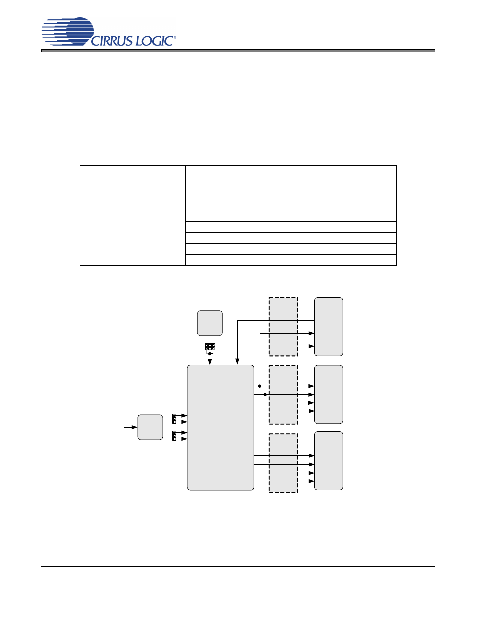
3.2.2
TDM In to TDM Out
The CS8422’s TDM output performance can be tested by setting the hardware switches as shown in
. This configures the digital clock and data signal routing on the board as shown in
TDM audio input data is provided by the TDM input header J30. The LRCK and SCLK signals located at
header J30 should be used to clock in the input TDM data. Optionally, digital AES3/EBU input can be pro-
vided by the XLR jack J19 to the RXP0 and RXN0 pins of the CS8422. The CS8422’s internal circuitry is
configured to multiplex the TDM input and AES3/EBU input data together and send the output data to se-
rial output port 1. This data is presented as TDM audio at header J24. The AES3/EBU input data is also
passed through (not multiplexed) to serial output port 2. This data is presented as PCM audio at header
J25. Refer to
for full details on hardware configuration.
Figure 13.
TDM In to TDM Out
Switch
Position
Setting
S3
MS_SEL[3:0]
1010
S4
SAOF[3:0]
1001
S7
RX_SELECT
0
TX_SELECT
0
TX_U/OUT SEL
0
NV/RERR SEL
0
V/AUDIO SEL
0
SRC MCK SEL
0
Table 2. Switch Settings - TDM In to TDM Out
CS8422
Buffer
Header
J24
Buffer
Header
J25
(MASTER)
(MASTER)
OSCLK1
OLRCK1
SDOUT1
OSCLK2
OLRCK2
SDOUT2
OSCLK2
OLRCK2
SDOUT2
OSCLK1
OLRCK1
SDOUT1
XTI
J23
Y1
Header
J30
TDM
OSCLK
TDM
OLRCK
TDM IN
Buffer
TDM
Out
TDM_IN
TDM
In
PCM Out
no SRC
RMCK
MCLK OUT
MCLK OUT
MCLK_OUT
J19
J21
AES3/EBU
In
J29
RXP0
RXP1
RXN0
RXN1