4 fpga register quick reference, 5 fpga register descriptions, 1 code revision id (address 01h) - read only – Cirrus Logic CDB8422 User Manual
Page 17: 2 mclk control (address 02h), Section 2.4, Section, Cdb8422
DS692DB2
17
CDB8422
2.4
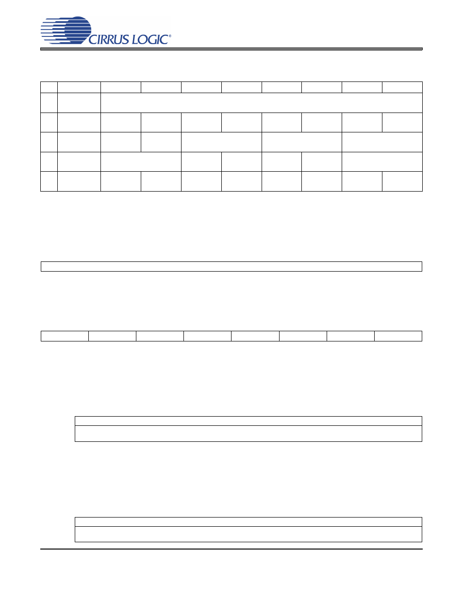
FPGA Register Quick Reference
This table shows the register names and their associated default values.
2.5
FPGA Register Descriptions
All registers are read/write unless otherwise stated. All “Reserved” bits must maintain their default state.
2.5.1
Code Revision ID (Address 01h) - Read Only
Function:
This register identifies the revision of the FPGA code. This register is read-only.
2.5.2
MCLK Control (Address 02h)
2.5.2.1 SAO2 HDR MCLK Source (SAO2_Mclk)
Default = 0
Function:
This bit controls the source of the MCLK signal sent to the SAO2 header J25. If the auxiliary source is
used, see
for options.
2.5.2.2 SAO1 HDR and CS8406 MCLK Source (SAO1_Mclk)
Default = 0
Function:
This bit controls the source of the MCLK signal sent to the SAO1 header J24 and the CS8406’s OMCK
pin. If the auxiliary source is used, see
for options.
Adr
Name
7
6
5
4
3
2
1
0
01h Rev_ID
RevID7
RevID6
RevID5
RevID4
RevID3
RevID2
RevID1
RevID0
x
x
x
x
x
x
x
x
02h Mclk_Ctl
Reserved
SAO2_Mclk SAO1_Mclk AUX_Mclk
Reserved
Reserved
Reserved
DUT_RST
0
0
0
0
0
0
0
1
03h Subclk_Ctl
TDM_SEL
Reserved
SAI_MS1
SAI_MS0
SAO2_MS1 SAO2_MS0 SAO1_MS1 SAO1_MS0
0
0
0
0
0
0
0
0
04h CS8406 Ctl 1
HWCK1
HWCK0
VBIT_IN
UBIT_IN
TCBL
CBIT_INT
SFMT1
SFMT0
0
0
0
0
0
0
0
0
05h CS8406 Ctl 2 Reserved
Reserved
Reserved
Reserved
Reserved
Reserved
8406_RST
AUDIOb
0
0
0
0
0
0
1
1
7
6
5
4
3
2
1
0
RevID7
RevID6
RevID5
RevID4
RevID3
RevID2
RevID1
RevID0
7
6
5
4
3
2
1
0
Reserved
SAO2_Mclk
SAO1_Mclk
AUX_Mclk
Reserved
HDR_AD1
HDR_AD0
DUT_RST
SAO2_Mclk Setting
SAO2 HDR MCLK Source
0 ..........................................CS8422 RMCK.
1 ..........................................AUX MCLK.
SAO1_Mclk Setting
SAO1 HDR and CS8406 MCLK Source
0 ..........................................CS8422 RMCK.
1 ..........................................AUX MCLK.