2 configuration options, 1 aes3/ebu in to s/pdif and pcm out, Figure 12.aes3/ebu in to s/pdif and pcm out – Cirrus Logic CDB8422 User Manual
Page 23: Section 3.2, Cdb8422
DS692DB2
23
CDB8422
3.2
Configuration Options
In hardware mode, to configure the CDB8422 for making performance measurements, one needs to use
the on-board control switches to set up the various components on the board. This section serves to give a
deeper understanding of the on-board circuitry and the digital clock and data signal routing involved in two
different hardware mode configurations of the CDB8422. These setups only serve as a starting point; the
switches can be further configured as needed (clock ratios, serial formats, etc).
3.2.1
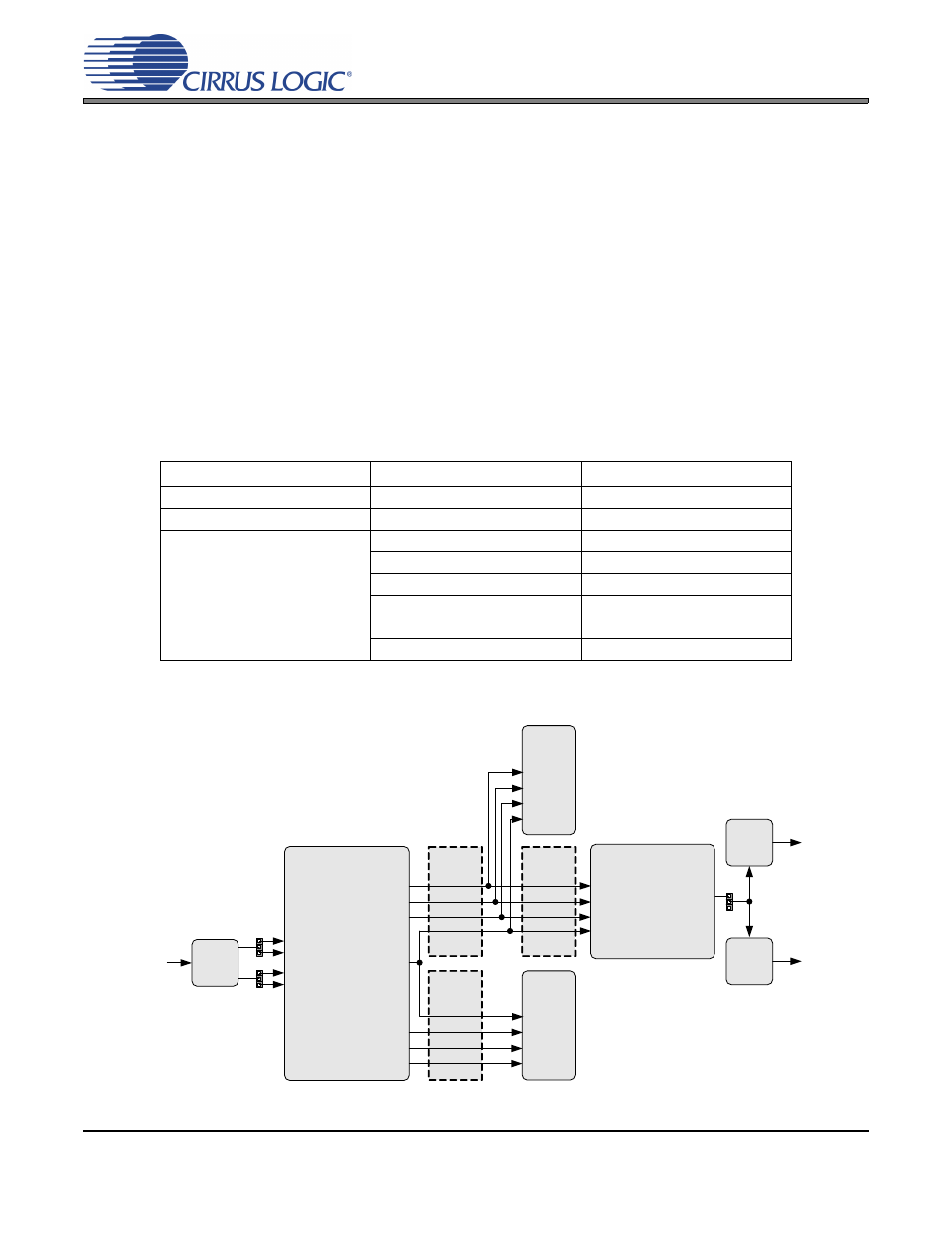
AES3/EBU In to S/PDIF and PCM Out
The CS8422’s AES3/EBU receiver and SRC output performance can be tested by setting the hardware
switches as shown in
. This configures the digital clock and data signal routing on the board as
shown in
Digital AES3/EBU input is provided by the XLR jack J19 to the RXP0 and RXN0 pins of the CS8422. The
CS8422’s internal circuitry is configured to send the input audio data through its SRC to serial output port
1. This data is presented as PCM audio at header J24 and S/PDIF audio at J27 (coaxial) and J28 (optical).
The input data is also passed through (SRC is bypassed) to serial output port 2. This data is presented
as PCM audio at header J25. Refer to
for full details on hardware configuration.
Figure 12. AES3/EBU In to S/PDIF and PCM Out
Switch
Position
Setting
S3
MS_SEL[3:0]
1010
S4
SAOF[3:0]
0011
S7
RX_SELECT
0
TX_SELECT
0
TX_U/OUT SEL
0
NV/RERR SEL
0
V/AUDIO SEL
0
SRC MCK SEL
1
Table 1. Switch Settings - AES3/EBU In to S/PDIF and PCM Out
CS8422
CS8406
S/PDIF Tx
(SLAVE)
Buffer
Buffer
Header
J24
Buffer
Header
J25
(MASTER)
(MASTER)
OSCLK1
OLRCK1
SDOUT1
OSCLK2
OLRCK2
SDOUT2
ISCLK
ILRCK
SDIN
OSCLK2
OLRCK2
SDOUT2
OSCLK1
OLRCK1
SDOUT1
Optical
S/PDIF
Out
J28
AND
J27
J31
Coaxial
S/PDIF
Out
S/PDIF
OUT
RMCK
OMCK
MCLK OUT
MCLK OUT
J19
J21
AES3/EBU
In
J29
RXP0
RXP1
RXN0
RXN1
PCM Out
through SRC
PCM Out
no SRC