Table 4. data to sdin1, 3 codec clock control (address 03h), Table 5. clocks to dac – Cirrus Logic CDB42448 User Manual
Page 18: Table 4. data to sdin1 table 5. clocks to dac, P 18
CDB42448
18
DS648DB2
5.2.4
SDIN1 MUX(SDINX.MUX)
Default = 10
Function:
This MUX selects the data lines from the CS8416, DSP Header, the ADC and the TDM Stream from
the TDMer (see Figure 4 on page 11).
5.3
CODEC CLOCK CONTROL (ADDRESS 03H)
5.3.1
DAC CLOCK MUX (DAC.CLK_MUX[1:0])
Default = 11
Function:
This MUX selects the sub-clock lines from the CS8416, ADC, DSP Header and the sub-clocks from
the TDMer internal to the FPGA (see Figure 3 on page 10).
5.3.2
FPGA CLOCKS TO DAC CLOCKS (FPGA->DAC)
Default = 0
0 - FPGA Masters DAC clock bus
1 - FPGA Slave to DAC clock bus
Function:
This bit toggles a control line for the internal clock buffer to the DAC serial port (see Figure 3 on page
10) .
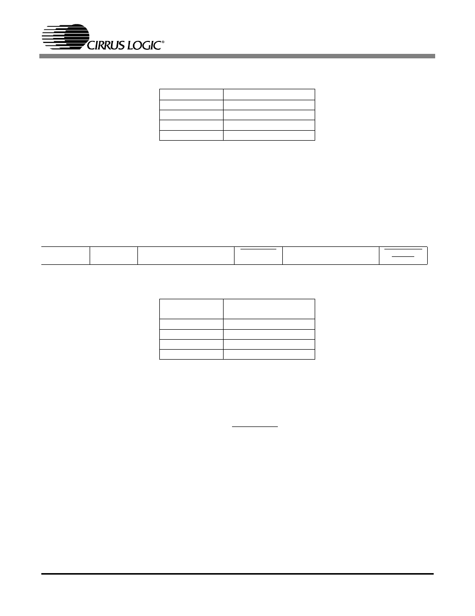
SDIN1.MUX[1:0]
Data Selection
00
CS8416 SDOUT
01
DSP_ SDOUT1
10
ADC_SDOUT1
11
TDM Stream
Table 4. Data to SDIN1
7
6
5
4
3
2
1
0
Reserved
Reserved
DAC.CLK_
MUX1
DAC.CLK_
MUX0
FPGA->DAC
ADC.CLK_
MUX1
ADC,CLK_
MUX0
FPGA->ADC-
CODEC
DAC.CLK_
MUX[1:0]
Clock Selection
00
CS8416
01
ADC
10
DSP DAC
11
TDMer
Table 5. Clocks to DAC