6 bypass control - advanced, Figure 7. bypass fpga control, Tion 3.6 provides details for routing clocks – Cirrus Logic CDB42448 User Manual
Page 14
CDB42448
14
DS648DB2
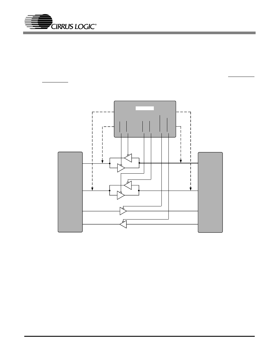
3.6
Bypass Control - Advanced
The DSP clocks and data may be routed through buffers directly to the CS42448, bypassing
the FPGA. This configuration may be desired for more stringent timing requirements at higher
clock speeds. See register “Bypass Control (address 06h)” on page 22. These bits are only
accessible through the Advanced tab of the Cirrus Logic FlexGui software.
NOTE: To avoid contention with the FPGA, set the clock direction for the FPGA appropriately: The FPGA->DAC
and FPGA->ADC bits in register 03h and 07h must be set to ‘1’b.
DSP Header
DSP_ADC.LRCK/
SCLK
DSP_DAC.LRCK/
SCLK
DSP.SDIN1-3
DSP.SDOUT1-4
CS42448
ADC.LRCK
/SCLK
DAC.LRCK
/SCLK
SDOUT1-3
SDIN1-4
FPGA – Bypass Control
D
S
P-
>D
AC
DS
P
->
A
DC
DA
C
->D
S
P
AD
C
->
D
SP
SD
OU
T
->
D
SP
D
SPD
AT
A
->D
A
C
Register 06h
NOTE: FPGA->DSPb bits in
Reg 07h must be disabled
to avoid bus contention.
NOTE: FPGA->ADC/
DACb bits in Reg 03h
must be disabled to avoid
bus contention.
Figure 7. Bypass FPGA Control