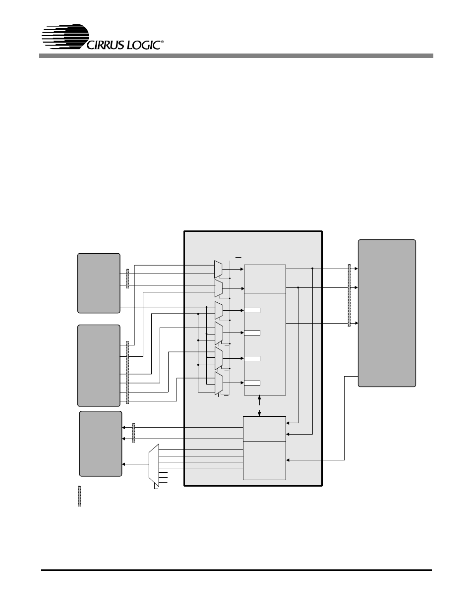
Figure 5. tdmer – Cirrus Logic CDB42448 User Manual
Page 12
CDB42448
12
DS648DB2
3.4.
Internal TDM Conversion, MUXing and Control (TDMer)
The graphical description below shows the routing topology of the TDM converter between the
CS42448, CS8416, CS8406 and DSP Header. Refer to register “TDM Conversion (address
01h)” on page 16 for configuration settings.
The TDMer allows the user to easily evaluate the CS42448 in the TDM digital interface format.
A 256Fs clock and an FS pulse is derived from either the CS8416 or DSP Header. Data is mul-
tiplexed onto one data line and transmitted to the DAC. Likewise, data from the ADC of the
CS42448 is de-multiplexed and transmitted to the CS8406. The CS8406 sub clocks, in this case,
must be taken from the TDM2PCM engine of the TDMer (refer to register “ADC or TDM2PCM
Clock Selection (T2P/ADC)” on page 20 for implementation).
The TDMer is also capable of transmitting the de-multiplexed data to the DSP Header; however,
the user must re-time this data using a DSP. The CDB42448 does not provide an option for rout-
ing the TDM2PCM clocks to the DSP Header.
PCM2TDM
Clocks
Data
CS8416
DSP.ADC_LRCK
DSP.ADC_SCLK
LRCK
SCLK
DSP Header
SDOUT
DSP.SDOUT1
DSP.SDOUT2
DSP.SDOUT3
DSP.SDOUT4
CS8406
LRCK
SCLK
SDIN
TDM2PCM
Clocks
Data
CS42448
DSP/CS8416
OUT1/OUT2
OUT1/OUT3
OUT1/OUT4
SDIN1
ADC/DAC_SCLK
ADC/DAC_LRCK
SDOUT1
CS8416_SCLK
CS8416_LRCK
DSP.ADC_LRCK
DSP.ADC_SCLK
DSP OUT1
CS8416_SDOUT
DSP OUT2
DSP OUT3
DSP OUT4
AUX
ADC3
ADC2
ADC1
= Other logic prior to input/output pin of FPGA not shown.
T2P_LRCK
T2P_SCLK
FS
256Fs SCLK
D_MUX[2:0]
TDM Stream
SDOUT1
SDOUT2
SDOUT3
AD
C
.SD
O
U
T
_
M
U
X
TDMer
MCLK
SLOT1
SLOT2
SLOT3
SLOT4
Figure 5. TDMer