Fpga register description, 1 tdm conversion (address 01h), P 16 – Cirrus Logic CDB42448 User Manual
Page 16
CDB42448
16
DS648DB2
5. FPGA REGISTER DESCRIPTION
All registers are read/write. See the following bit definition tables for bit assignment information. The de-
fault state of each bit after a power-up sequence or reset is listed in each bit description.
5.1
TDM CONVERSION (ADDRESS 01H)
5.1.1
PCM2TDM CLOCK SELECTION (DSP/CS8416)
Default = 0
0 - CS8416
1- DSP_ADC Header
Function:
This bit selects the clock source for the PCM2TDM (P2T) converter. It also selects the data source
for Slot 1 (see Figure 5 on page 12) of the TDMer.
This bit also serves as the MSB of the 3:2 data selection MUX’s for slots 2-4 of the TDM Stream (see
Figure 5 on page 12).
5.1.2
PCM2TDM DATA SELECTION (OUT1/OUTX)
Default = 0
0 - OUTx
1- OUT1
Function:
This bit selects the data source for the PCM2TDM (P2T) converter. The DSP/CS8416 bit serves as
the MSB of the MUX that selects between OUTx and OUT1.
If the CS8416 is selected as the clock source for the P2T converter, this bit is ignored and the CS8416
SDOUT will be selected as the data source for slots 2-4 (see Figure 5 on page 12).
5.1.3
POWER DOWN TDM CONVERTER (PDN_TDMER)
Default = 0
0 - Disabled
1- Enabled
Function:
This bit powers down the TDMer.
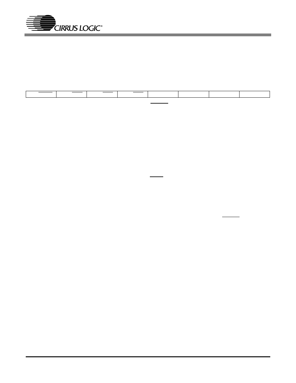
7
6
5
4
3
2
1
0
DSP/CS8416
OUT1/OUT2
OUT1/OUT3
OUT1/OUT4
Reserved
Reserved
Reserved
PDN_TDMer