3 design process, 1 operating parameters, An368 – Cirrus Logic AN368 User Manual
Page 9: Output power p, Ac line input voltage v, Channel 1 secondary output voltage v, Channel 2 secondary output voltage v, Channel 1 load current i, Channel 2 load current i, Maximum switching frequency
AN368
AN368REV2
9
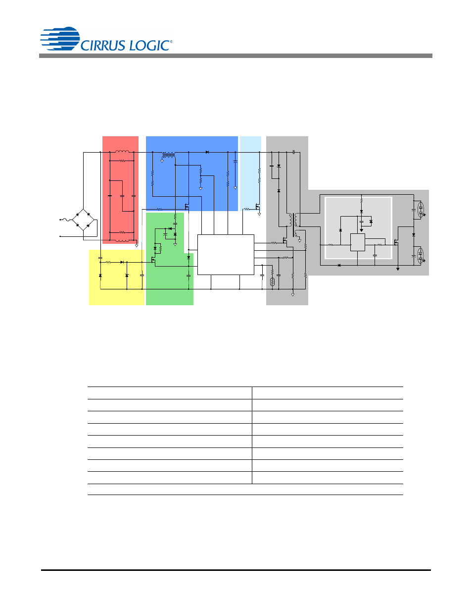
3 Design Process
The design process for a two-stage power converter system can be partitioned into seven circuit blocks (see
Figure 1). The AC line voltage is passed through an electromagnetic interference (EMI) filter to prevent injection of
switching noise from the driver into the power line. The output of the EMI filter is then converted to the desired DC
output by a boost PFC followed by a flyback converter. The second stage is an isolated flyback circuit that requires
a phase synchronizer to control the two-channel output currents. The power converter system includes the Gate Bi-
as, Steady State Supply, and Active Clamp support circuitry.
3.1 Operating Parameters
To initiate the design procedure, a set of operating parameters is required. Operating parameters required for
the analytical process are outlined in the table below. Parameters critical to the overall design, but not
specifically addressed in this document, include EMI compliance, efficiency, form factor, layout, and operating
temperature.
Parameter
Symbol
Output Power
P
OUT
AC Line Input Voltage
V
IN
Channel 1 Secondary Output Voltage
V
CH1
Channel 2 Secondary Output Voltage
V
CH2
Channel 1 Load Current
I
CH1
Channel 2 Load Current
I
CH2
Maximum Switching Frequency
*
F
sw(max)
* Increasing F
sw
may reduce the size of the magnetics but increases switching losses in the FET.
TX1
Z3
L1
L3
R14
R6
R7
R13
R8
R1
Q2
L2
Z2
C23
D7
D2
Q4
Q1
D3
R17
R18
R22
R23
Q5
R21
R27
R5
BR1
F1
R33
D8
R36
CS1630 /31
IAC
FBAUX
BSTOUT
CLAMP
GD
FBSENSE
eOTP
VDD
SOURCE
CY
D2
L
N
AC Mains
D1
R25
R9
R11
R24
D4
BSTAUX
R24
Boost
Gate Bias
Steady State
Supply
Active
Clamp
Second Stage
Flyback
EMI
C11
C17
C12
C5
C9
C11
C6
C1
C4
C13
R3
D6
U2
C10
C8
C15
D5
D
GND
_
Q
V CC
D15
R12
D10
Q3
R2
C16
SGND
GND
GND
IGND
C24
R29
NTC
D9
Phase
Sync
Figure 1. Diagram of CS1630 Design
Driving Two LED Strings in Series