3 design procedure, An368, Figure 2. flyback series output model – Cirrus Logic AN368 User Manual
Page 11
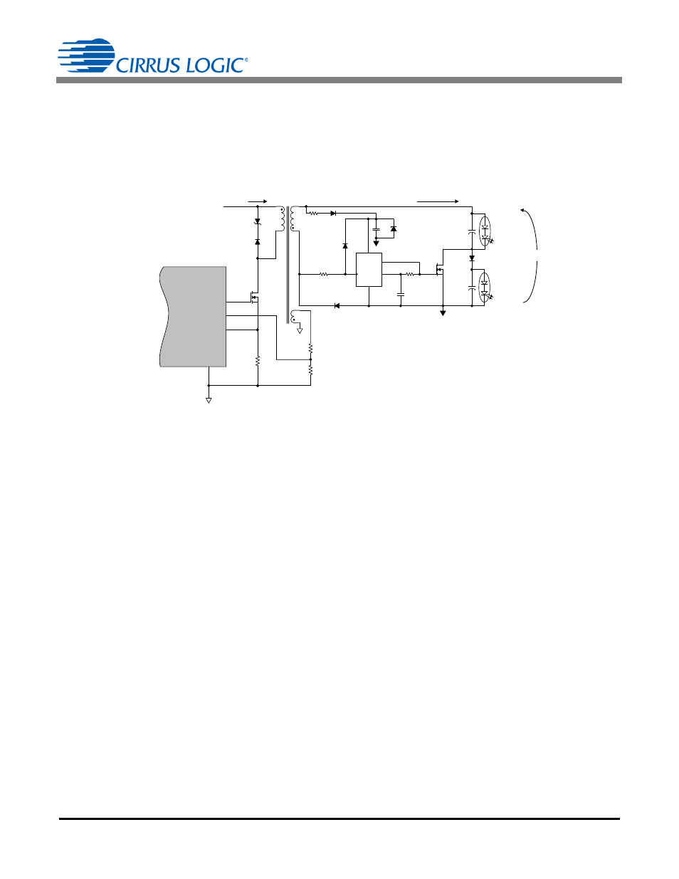
AN368
AN368REV2
11
3.3 Design Procedure
Step 1) Select Input Voltage
The CS1630 is optimized for 120VAC line voltage applications and designs targeting 108 to 132 VAC markets.
Step 2) Design for a Flyback Topology
The light engine is defined for a flyback topology in a series configuration. Figure 2 illustrates a flyback
topology with a series lamp configuration.
This document focuses on designing and programming a driver with a flyback topology in a series
configuration. Cirrus Logic, Inc. and its affiliates and subsidiaries generally make no representations or
warranties that the combination of Cirrus Logic’s products with light-emitting diodes (“LEDs”), converter
materials, and/or other components will not infringe any third-party patents, including any patents related to
color mixing in LED lighting applications, such as, for example, U.S. Patent No. 7,213,940 and related patents
of Cree, Inc. For more information, please see Cirrus Logic’s Terms and Conditions of Sale, or contact a Cirrus
Logic sales representative.
a. Set OTP for a Series Configuration
The two LED strings are arranged in series so that current passes through either one or both LED strings. A
MOSFET is used to shunt current around one string on alternating switching cycles. In this configuration, one
string is required to have a larger output current than the other string.
When considering a series design, it is recommended that the current flowing through one of the LED channels
be 80% or lower than that of the other LED channel at all times. The LED string that has current flowing
continuously is referred to as channel 1 LED (I
CH1
), while the string with the bypass FET is referred to as
channel 2 LED (I
CH2
); I
CH2
0.8
I
CH1
. A good rule of thumb is that channel 2 LED must always have a forward
voltage of 85% or lower than channel 1 LED.
The LED_ARG bit in register Config3 at Address 35 selects which channel is connected to the color LED string.
When bit LED_ARG is set to ‘1’, the color LED string is connected to channel 2.
The STRING bit in register Config3 at Address 35 selects the second-stage output channel configuration.
When bit STRING is set to ‘1’, a series configuration is selected.
b. Selecting a Flyback Topology
Flyback topology is enabled by setting bit S2CONFIG to ‘1’ in register Config12 at Address 44. The flyback
transformer input-to-output voltage ratio is used to determine the duty cycle and minimum turn ‘ON’ switching
period T1 for the power FET. The flyback transformer is designed as an isolated topology, and the digital
synchronization signal needs to be disabled. Set bit SYNC in register Config4 at Address 36 to ‘0’. Since bit
S2CONFIG is configured for a flyback topology, bits BUCK[3:0] in register Config10 at Address 42 are ignored
by the digital algorithm.
D2
R22
Z3
R21
R23
Q5
CS1630 /31
FBAUX
GND
13
GD
FBSENSE
15
12
11
TX1
V
B S T
R3
D6
U2
C10
C8
C15
D5
D
GND
_
Q
V CC
D15
R12
D10
Q3
R2
C16
Channel 1 LED
(White)
Channel 2 LED
(Red)
GND
IGND
I
MODE x
I
P RI
V
MODE x
D9
Figure 2. Flyback Series Output Model