E. t2 commutation time delay compensation, An368 – Cirrus Logic AN368 User Manual
Page 30
AN368
30
AN368REV2
e. T2 Commutation Time Delay Compensation
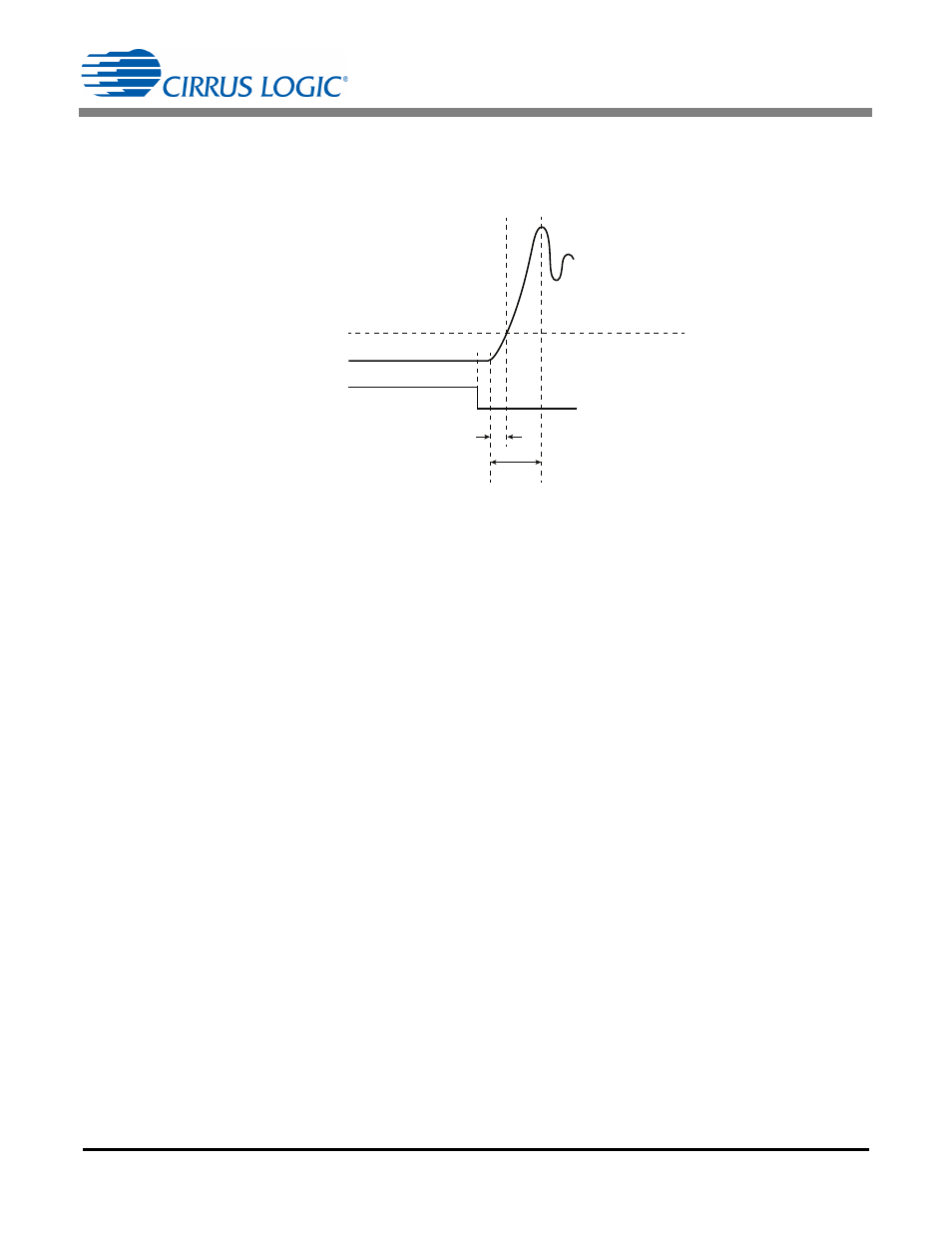
The presence of circuit parasitic components, such as leakage inductance, causes a delay between the time
the primary current becomes zero and the power actually being transferred to the load. This delay is shown in
the following illustration:
T2 commutation time delay is enabled by programming bit T2COMP in register Config2 at Address 34. The T2
commutation time delay compensation is designed for a flyback stage with a large commutation time delay
between the fall of the primary current and the rise of the secondary current during the switching cycle.
Since the output current is given by Equations 27 and 28, this delay can cause errors in current regulation. The
CS1630 can compensate for this delay using the following steps:
1. Measure the time difference T
dt2
between the time the gate turns ‘OFF’ and the time the signal applied
to pin FBAUX reaches 200 mV.
2. Measure the time difference T
dt2
between the time the gate turns ‘OFF’ and the time the signal applied
to pin FBAUX reaches its maximum ringing value.
3. Calculate Mode 1 time T2 compensation gain T2
CH1CompGain
using Equation 54:
where bits T2CH1GAIN[5:0] in register Config4 at Address 36 are configured using Equation 55:
4. Repeat the above process for Mode 2. Calculate Mode 2 time T2 compensation gain T2
CH2CompGain
using Equation 56:
where bits T2CH2GAIN[5:0] in register Config17 at Address 49 are configured using Equation 57:
T
dt2’
T
dt2
FBAUX
Point at which pin
FBAUX equals 200mV
GD
Figure 12. Point at which the Voltage Applied to Pin FBAUX is 200mV
[Eq. 54]
T2
CH1CompGain
0.0625 T
2CH1GAIN[5:0]
=
[Eq. 55]
T2CH1GAIN[5:0]
T
dt2
T
dt2
-----------
=
[Eq. 56]
T2
CH2CompGain
0.0625 T
2CH2GAIN[5:0]
=
[Eq. 57]
T2CH2GAIN[5:0]
T
dt2
T
dt2
-----------
=