4 design example, 1 design steps, An368 – Cirrus Logic AN368 User Manual
Page 52
AN368
52
AN368REV2
4 Design Example
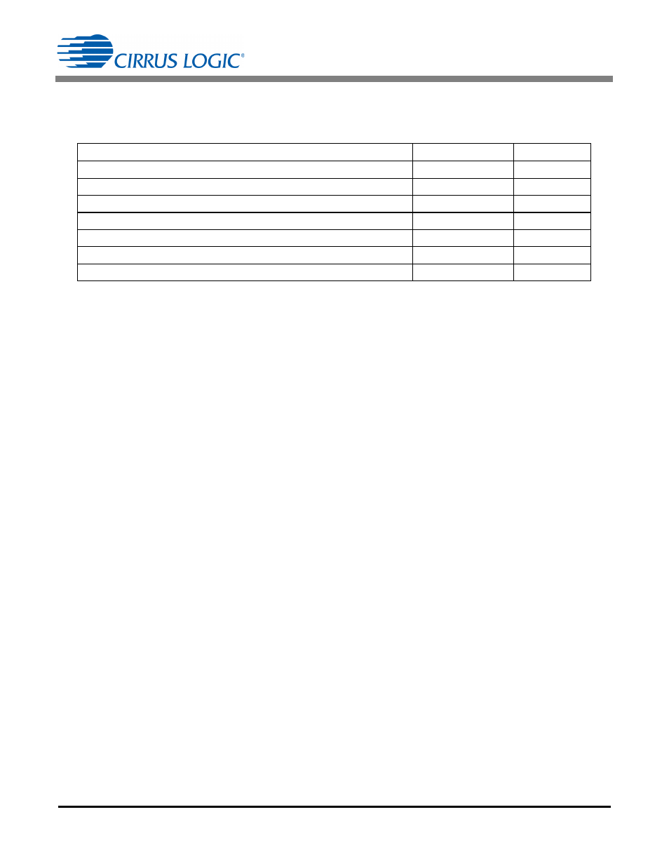
The Cirrus Logic CRD1630-9W reference design is used for the design example. The required operating parameters
for the analytical process are outlined in the following table.
4.1 Design Steps
Step 1) Select Input Voltage
The CS1630 is selected and optimized for 120V applications.
Step 2) Design for a Flyback Topology
a. Set OTP for a Series Configuration
A series configuration is selected and the IC is configured using the OTP setting in the following steps:
1. Configure which channel is connected to the color LED string. The color LED string is connected to
channel 2, and bit LED_ARG is set to ‘1’. Bit LED_ARG is bit 4 in register Config3 at Address 35.
2. Configure second-stage output channel configuration. The white and color LED strings are connected
in a series configuration, and bit STRING is set to ‘1’. Bit STRING is bit 7 in register Config3 at Address
35.
b. Selecting a Flyback Topology
A flyback topology is selected and the IC is configured using the OTP setting in the following steps:
1. Configure the second stage for a isolated flyback transformer. Bit S2CONFIG is set to ‘1’. Bit S2CONFIG
is bit 5 in register Config12 at Address 44.
2. Bits BUCK[3:0] in register Config10 at Address 42 do not apply to example design.
3. Disable the digital synchronization signal by setting bit SYNC in register Config4 at Address 36 to ‘0’.
Step 3) Determine Second-stage Parameters for a Flyback Topology
a. Set the Value for Boost Output Voltage
The boost output voltage V
BST
is determined by an internal parameter and changes slightly depending on the
type of dimmer detected. Sense resistors R7, R8, R14, and R15 are set to 750k
each, and the resulting V
BST
is approximately 200V for a 120V system. V
BST
is regulated by charging the boost output capacitor to its
nominal value each half line-cycle. V
BST
droops to its lowest value towards the end of each half line-cycle until
the boosting process starts again in the next half line-cycle.
b. Select an Appropriate FET
Use Equation 2
to c
alculate the maximum boost output voltage V
BST(max)
. The CS1630 limits the boost output
voltage to +10%. V
BST(max)
is calculated using Equation 81:
Using a 300V zener as a clamp device sets the maximum zener clamp voltage V
Zener
to 315V (+5%
tolerance), leaving 65V of V
Margin
to a 600V FET. Using an analytical approach to partition V
Zener
into
V
Reflected
and (V
Reflected
- V
Zener
) requires assumptions about the switching details.
Parameter
Symbol
Value
Output Power
P
OUT
7.0W
AC Line Voltage (nominal)
V
IN
120V
Channel 1 Output Voltage
V
CH1
9.7V
Channel 2 Output Voltage
V
CH2
10.3V
Channel 1 Load Current
I
CH1
488mA
Channel 2 Load Current
I
CH2
213mA
Maximum Channel 1 Switching Frequency
*
F
sw1(max)
70kHz
* Increasing F
sw
reduces the size of the magnetics but increases switching losses in the FET.
V
BST max
200
=
1.1
220V
=
[Eq. 81]