Precision voltage generator offset voltage, Da1855a differential amplifier – Teledyne LeCroy DA1855A User Manual
Page 24
DA1855A Differential Amplifier
18
922258-00 Rev A
Precision Voltage Generator Offset Voltage
The rear panel OFFSET VOLTAGE BNC (PVG) output connector, is a monitor of the Precision Voltage
Generator (PVG). The voltage present on this connector is the same voltage as that applied to the –
INPUT when the –INPUT coupling is set to VCOMP or internally to the DA1855A when VDIFF is
selected. The OFFSET VOLTAGE output can be used to monitor the PVG with a digital Voltmeter
(DVM). A low pass filter between the PVG output and the –INPUT removes radio frequency
interference (RFI) from the signal. This filter does not attenuate the PVG signal.
The PVG output is not attenuated by the input attenuator or probes, whereas the input signal is.
Therefore the effective range of V
COMP
is increased by a factor of 10 when the ÷10 ATTENUATOR is
selected or a ÷10 attenuating probe is used to attenuate the input signal. The PVG numerical display
reflects the attenuator setting and probe attenuation when the probe is readout encoded. As an
example, if there are no probes attached, the ÷10 ATTENUATOR is selected and the display is set to
read –155.000, the PVG output will actually be –15.5 Volt.
The decimal in the display will be in the correct location to indicate the voltage at the PVG output
when no probes are attached and ÷1 ATTENUATOR and X1 GAIN are selected.
The OFFSET VOLTAGE BNC (PVG) output also presents the same voltage used internally for
differential offset when V
DIFF
is selected. Because the PVG is applied to the amplifier to create a true
differential offset, the relationship between V
DIFF
and the voltage at the OFFSET VOLTAGE BNC (PVG)
output (changes with the amplifier gain selection according to the following table:
The maximum V
DIFF
is multiplied by any probe attenuation factor. The DA1855A front panel displays
the correct offset referred to the instrument input.
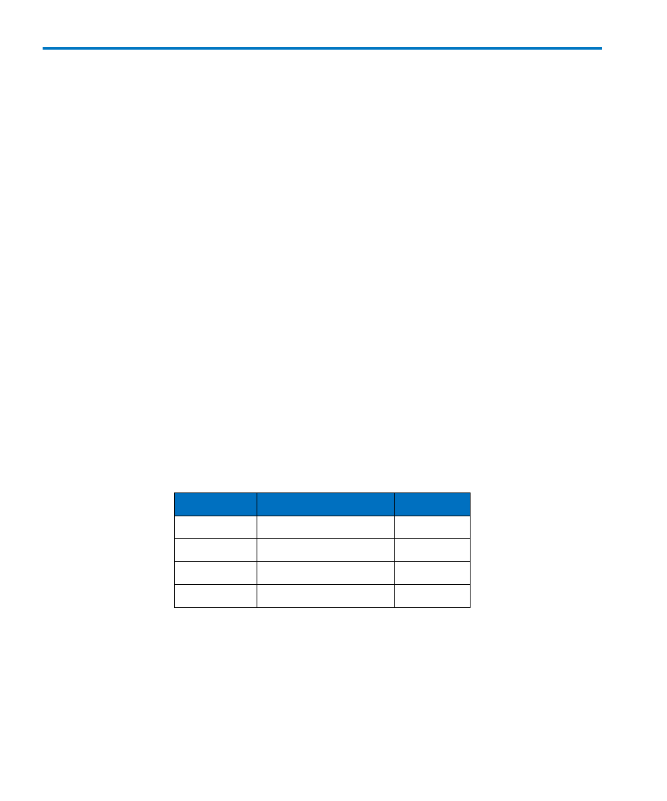
Table 1, V
DIFF
Range for Different Gain and Attenuator Settings
Gain
Attenuation Max.
V
DIFF
X1
÷1
± 10 V
X1
÷10
± 100 V
X10
÷1
± 1 V
X10
÷10
± 10 V
When using readout encoded probes which the DA1855A senses, the PVG readout calculates the
effective differential offset at the probe tip. Of course, both probes must have the same attenuation
factor.
In the V
COMP
mode, the maximum OFFSET VOLTAGE input is limited by the DA1855A common mode
dynamic range. In the V
DIFF
mode it is limited by the dynamic range of the internal V
DIFF
amplifier.