Block diagram, Port 1 port 2 – Atec Anritsu-MS4640B User Manual
Page 40
40
PN: 11410-00611 Rev. A
MS4640B Series TDS
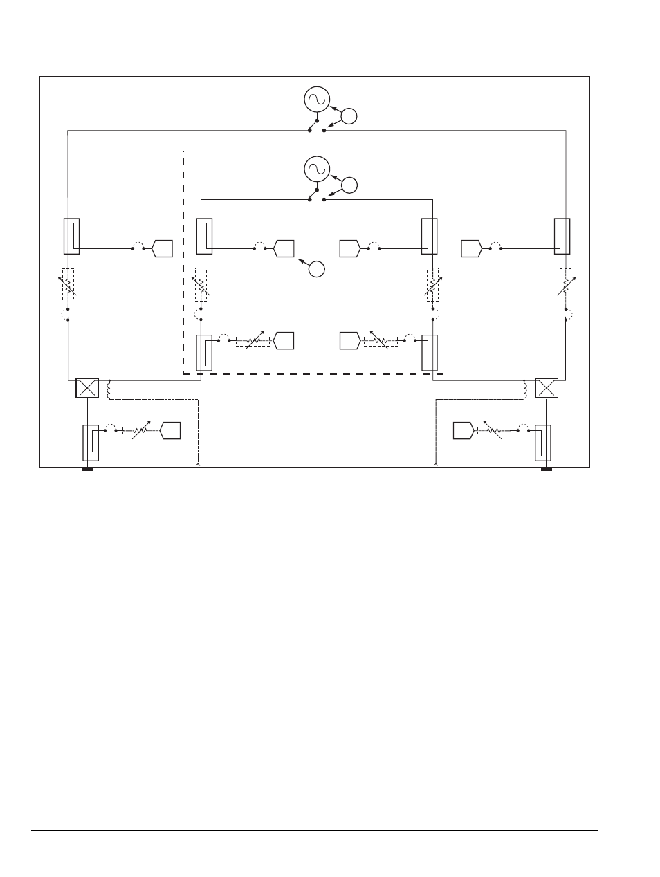
Block Diagram
VectorStar™ MS4640B Series
Block Diagram
A. With Option 031 Dual Source Architecture, second low-band and high-band sources are added and the two switches are removed. One set of sources
is dedicated to each of the VNA test port paths.
B. With Option 035 IF Digitizer, high speed digitizers are added to the receiver paths (a
1
, b
1
, a
2
, b
2
) for fast IF detection.
MS4640B Series VNA Block Diagram – Fully Loaded Configuration
> 2.5 GHz
High Band
< 2.5 GHz
Low Band
Port 1
Port 2
Bias 1
a
1
a
1
a
2
a
2
b
1
b
1
b
2
b
2
Bias 2
A
A
B
Optional
See also other documents in the category Atec Equipment:
- Anritsu-PIM-MW82119A (2 pages)
- Boonton-PIM31 (6 pages)
- AWT-PIM-S1L-Tetra Series (2 pages)
- AWT-PIM-S1P Series (2 pages)
- AWT-PIM-S1L Series (2 pages)
- AWT-PIM-Expandable Series (2 pages)
- AWT-PIM-Single Series (2 pages)
- CCI-PimPro (4 pages)
- JDSU-FST-2310 (10 pages)
- JDSU-T-Berd-6000 (8 pages)
- Agilent-N9912A (2 pages)
- Agilent-E5515C (4 pages)
- Agilent-E4406A (20 pages)
- Agilent-N4010A (16 pages)
- Anritsu-S412E (19 pages)
- Anritsu-S810D-S820D (2 pages)
- Anritsu-S820E (16 pages)
- Anritsu-MT8221B (28 pages)
- Anritsu-MT8221B (24 pages)
- Anritsu-S412D (16 pages)
- Anritsu-MT8222A (8 pages)
- Anritsu-MT8220T (28 pages)
- Anritsu-MT8212E-MT8213E (32 pages)
- Anritsu-S332D-31D (12 pages)
- Anritsu-MT8212A (2 pages)
- Bird-SA Series (2 pages)
- Anritsu-S331E-S332E-S361E-S362E (16 pages)
- Anritsu-S331L (12 pages)
- Advantest-Q8163 (1 page)
- Agilent-83557A-83558A (4 pages)
- Agilent-11896A (5 pages)
- Agilent-8169A (6 pages)
- Agilent-81689A_B-81649A (6 pages)
- Agilent-8163A-81634A (8 pages)
- Agilent-81624B (11 pages)
- Agilent-81618A (112 pages)
- Agilent-8703A (16 pages)
- Agilent-8156A (8 pages)
- Advanced-Fiber-Solutions-OLK51 Series (5 pages)
- Anritsu_MS9720A (12 pages)
- Anritsu-ML9001A (4 pages)
- Corning-Optivisor400 (6 pages)
- Anritsu_CMA5000a (4 pages)
- Agilent-E6008B (12 pages)
- AFL-Noyes-FLX3 (6 pages)