Absolute maximum ratings, Electrical characteristics – Rainbow Electronics MAX3942 User Manual
Page 2
MAX3942
10Gbps Modulator Driver
2
_______________________________________________________________________________________
ABSOLUTE MAXIMUM RATINGS
Stresses beyond those listed under “Absolute Maximum Ratings” may cause permanent damage to the device. These are stress ratings only, and functional
operation of the device at these or any other conditions beyond those indicated in the operational sections of the specifications is not implied. Exposure to
absolute maximum rating conditions for extended periods may affect device reliability.
Supply Voltage V
EE
..............................................-6.0V to +0.5V
Voltage at MODEN,
RTEN, PLRT, MODSET............................(V
EE
- 0.5V) to +0.5V
Voltage at DATA+, DATA-, CLK+, and CLK-……-1.65V to +0.5V
Voltage at OUT+, OUT- ................................……….-4V to +0.5V
Voltage at PWC+, PWC- ...................(V
EE
- 0.5V) to (V
EE
+ 1.7V)
Continuous Power Dissipation (T
A
= +85°C)
24-Pin Thin QFN (derate 20.8mW/° above +85°C) ....1354mW
Current into or out of OUT+, OUT-.................……………...80mA
Storage Temperature Range .....................……-55°C to +150°C
Operating Temperature Range ....................……-40°C to +85°C
Lead Temperature (soldering, 10s)............………………+300°C
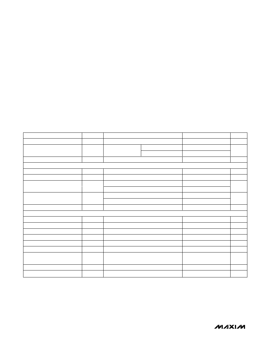
ELECTRICAL CHARACTERISTICS
(V
EE
= -5.5V to -4.9V, T
A
= -40°C to +85°C. Typical values are at V
EE
= -5.2V, I
MOD
= 100mA, and T
A
= +25°C, unless otherwise noted.)
PARAMETER
SYMBOL
CONDITIONS
MIN
TYP
MAX
UNITS
Power-Supply Voltage
V
EE
-5.5
-4.9
V
Retime disabled
125
175
Supply Current
I
EE
Excluding I
MOD
(Note 1)
Retime enabled
140
200
mA
Power-Supply Noise Rejection
PSNR
f
≤ 2MHz (Note 2); see Figure 3
15
dB
SIGNAL INPUT (Note 3)
Input Data Rates
NRZ
10.7
Gbps
Single-Ended Input Resistance
R
IN
Input to GND
42.5
50
58.5
Ω
DC-coupled, Figure 1a
-1
0
Single-Ended Input Voltage
V
IS
AC-coupled, Figure 1b
-0.4
+0.4
V
DC-coupled (Note 4)
0.2
2.0
Differential Input Voltage
V
ID
AC-coupled (Note 4)
0.2
1.6
V
P-P
Differential Input Return Loss
RL
IN
≤ 15GHz
15
dB
MODULATION (Note 5)
Maximum Modulation Current
112
120
mA
P-P
Minimum Modulation Current
V
MODSET
= V
EE
37
40
mA
P-P
MODSET Voltage Range
V
MODSET
V
EE
V
EE
+ 1
V
E q ui val ent M od ul ati on Resi stance
R
MODEQV
(Note 7)
11.1
Ω
Modulation Set Bandwidth
Modulation depth 10%, 50
Ω driver load
5
MHz
MODSET Input Resistance
20
k
Ω
Modulation-Current Temperature
Stability
(Note 6)
-980
0
ppm/
°C
Modulation-Current-Setting Error
50
Ω driver load, T
A
= +25
°C
-10
+10
%
Output Resistance
R
OUT
OUT+ and OUT- to GND
42.5
50
58.5
Ω