External interrupt flag register – eifr, Pin change mask register – pcmsk, Attiny2313 – Rainbow Electronics ATtiny2313 User Manual
Page 63
63
ATtiny2313
2543A–AVR–08/03
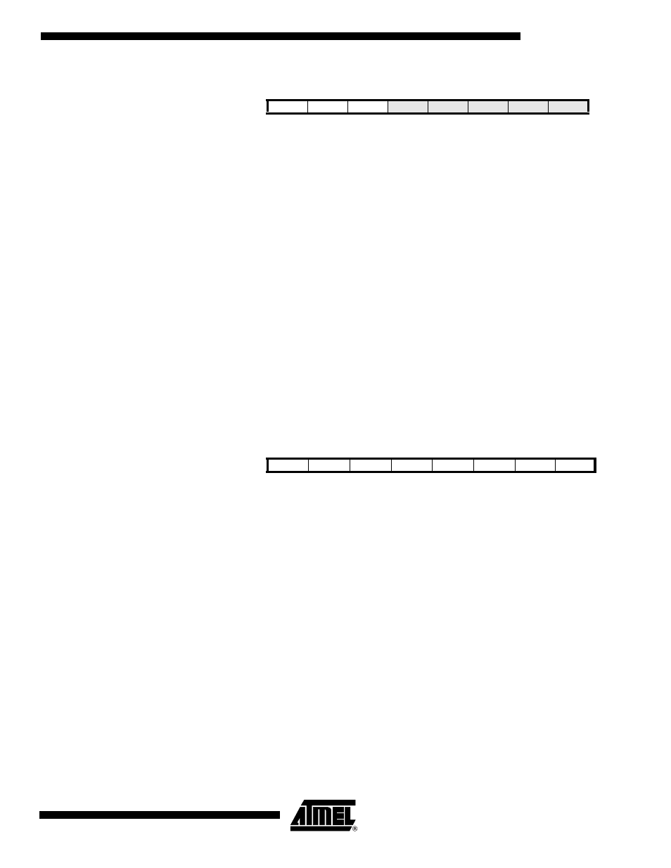
External Interrupt Flag
Register – EIFR
• Bit 7 – INTF1: External Interrupt Flag 1
When an edge or logic change on the INT1 pin triggers an interrupt request, INTF1
becomes set (one). If the I-bit in SREG and the INT1 bit in GIMSK are set (one), the
MCU will jump to the corresponding Interrupt Vector. The flag is cleared when the inter-
rupt routine is executed. Alternatively, the flag can be cleared by writing a logical one to
it. This flag is always cleared when INT1 is configured as a level interrupt.
• Bit 6 – INTF0: External Interrupt Flag 0
When an edge or logic change on the INT0 pin triggers an interrupt request, INTF0
becomes set (one). If the I-bit in SREG and the INT0 bit in GIMSK are set (one), the
MCU will jump to the corresponding Interrupt Vector. The flag is cleared when the inter-
rupt routine is executed. Alternatively, the flag can be cleared by writing a logical one to
it. This flag is always cleared when INT0 is configured as a level interrupt.
• Bit 5 – PCIF: Pin Change Interrupt Flag
When a logic change on any PCINT7..0 pin triggers an interrupt request, PCIF becomes
set (one). If the I-bit in SREG and the PCIE bit in GIMSK are set (one), the MCU will
jump to the corresponding Interrupt Vector. The flag is cleared when the interrupt routine
is executed. Alternatively, the flag can be cleared by writing a logical one to it.
Pin Change Mask Register –
PCMSK
• Bit 7..0 – PCINT7..0: Pin Change Enable Mask 15..8
Each PCINT7..0-bit selects whether pin change interrupt is enabled on the correspond-
ing I/O pin. If PCINT7..0 is set and the PCIE bit in GIMSK is set, pin change interrupt is
enabled on the corresponding I/O pin. If PCINT7..0 is cleared, pin change interrupt on
the corresponding I/O pin is disabled.
Bit
7
6
5
4
3
2
1
0
INTF1
INTF0
PCIF
–
–
–
–
–
EIFR
Read/Write
R/W
R/W
R
R
R
R
R
R/W
Initial Value
0
0
0
0
0
0
0
0
Bit
7
6
5
4
3
2
1
0
PCINT7
PCINT6
PCINT5
PCINT4
PCINT3
PCINT2
PCINT1
PCINT0
PCMSK
Read/Write
R/W
R/W
R/W
R/W
R/W
R/W
R/W
R/W
Initial Value
0
0
0
0
0
0
0
0