Digital input disable register – didr, Attiny2313 – Rainbow Electronics ATtiny2313 User Manual
Page 152
152
ATtiny2313
2543A–AVR–08/03
ing the corresponding interrupt handling vector. Alternatively, ACI is cleared by writing a
logic one to the flag.
• Bit 3 – ACIE: Analog Comparator Interrupt Enable
When the ACIE bit is written logic one and the I-bit in the Status Register is set, the Ana-
log Comparator interrupt is activated. When written logic zero, the interrupt is disabled.
• Bit 2 – ACIC: Analog Comparator Input Capture Enable
When written logic one, this bit enables the input capture function in Timer/Counter1 to
be triggered by the Analog Comparator. The comparator output is in this case directly
connected to the input capture front-end logic, making the comparator utilize the noise
canceler and edge select features of the Timer/Counter1 Input Capture interrupt. When
written logic zero, no connection between the Analog Comparator and the input capture
function exists. To make the comparator trigger the Timer/Counter1 Input Capture inter-
rupt, the ICIE1 bit in the Timer Interrupt Mask Register (TIMSK) must be set.
• Bits 1, 0 – ACIS1, ACIS0: Analog Comparator Interrupt Mode Select
These bits determine which comparator events that trigger the Analog Comparator inter-
rupt. The different settings are shown in Table 63.
When changing the ACIS1/ACIS0 bits, the Analog Comparator Interrupt must be dis-
abled by clearing its Interrupt Enable bit in the ACSR Register. Otherwise an interrupt
can occur when the bits are changed.
Digital Input Disable Register
– DIDR
• Bit 1, 0 – AIN1D, AIN0D: AIN1, AIN0 Digital Input Disable
When this bit is written logic one, the digital input buffer on the AIN1/0 pin is disabled.
The corresponding PIN Register bit will always read as zero when this bit is set. When
an analog signal is applied to the AIN1/0 pin and the digital input from this pin is not
needed, this bit should be written logic one to reduce power consumption in the digital
input buffer.
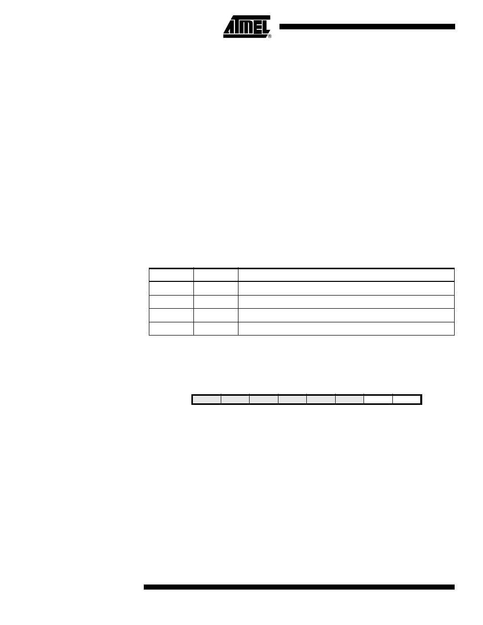
Table 63. ACIS1/ACIS0 Settings
ACIS1
ACIS0
Interrupt Mode
0
0
Comparator Interrupt on Output Toggle.
0
1
Reserved
1
0
Comparator Interrupt on Falling Output Edge.
1
1
Comparator Interrupt on Rising Output Edge.
Bit
7
6
5
4
3
2
1
0
–
–
–
–
–
–
AIN1D
AIN0D
DIDR
Read/Write
R
R
R
R
R
R
R/W
R/W
Initial Value
0
0
0
0
0
0
0
0