Mcu control register – mcucr, Alternate functions of port a, Alternate functions of port b – Rainbow Electronics ATtiny2313 User Manual
Page 54: Attiny2313
54
ATtiny2313
2543A–AVR–08/03
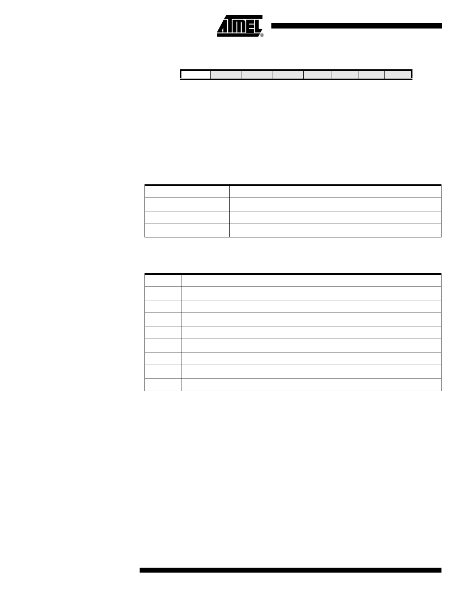
MCU Control Register –
MCUCR
• Bit 7 – PUD: Pull-up Disable
When this bit is written to one, the pull-ups in the I/O ports are disabled even if the DDxn
and PORTxn Registers are configured to enable the pull-ups ({DDxn, PORTxn} = 0b01).
See “Configuring the Pin” on page 48 for more details about this feature.
Alternate Functions of Port A
The Port A pins with alternate functions are as shown in Table 5.
Alternate Functions of Port B
The Port B pins with alternate functions are shown in Table 26.
The alternate pin configuration is as follows:
• USCK/SCL/PCINT7 - Port B, Bit 7
USCK: Three-wire mode Universal Serial Interface Clock.
SCL: Two-wire mode Serial Clock for USI Two-wire mode.
PCINT7: Pin Change Interrupt source 7. The PB7 pin can serve as an external interrupt
source.
• DO/PCINT6 - Port B, Bit 6
DO: Three-wire mode Universal Serial Interface Data output. Three-wire mode Data out-
put overrides PORTB6 value and it is driven to the port when data direction bit DDB6 is
set (one). However the PORTB6 bit still controls the pull-up enabling pull-up, if direction
is input and PORTB6 is set (one).
Bit
7
6
5
4
3
2
1
0
PUD
SM1
SE
SM0
ISC11
ISC10
ISC01
ISC00
MCUCR
Read/Write
R/W
R/W
R/W
R/W
R/W
R/W
R/W
R/W
Initial Value
0
0
0
0
0
0
0
0
Table 25. Port A Pins Alternate Functions
Port Pin
Alternate Function
PA2
RESET, dW
PA1
XTAL2
PA0
XTAL1
Table 26. Port B Pins Alternate Functions
Port Pin
Alternate Functions
PB7
USCK/SCL/PCINT7
PB6
DO/PCINT6
PB5
DI/SDA/PCINT5
PB4
OC1B/PCINT4
PB3
OC1A/PCINT3
PB2
OC0A/PCINT2
PB1
AIN1/PCINT1
PB0
AIN0/PCINT0