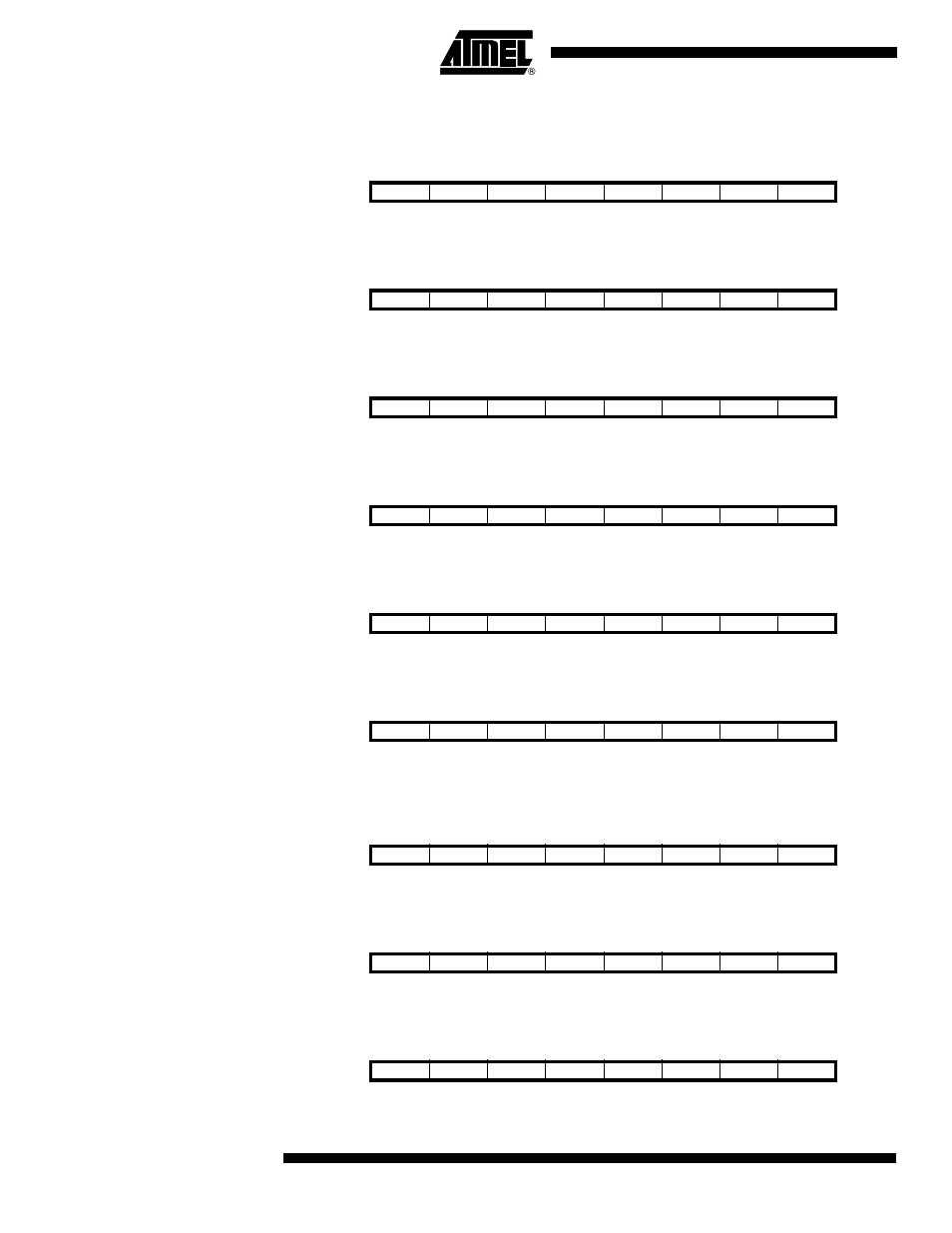
Register description for i/o-ports, Port a data register – porta, Port a data direction register – ddra – Rainbow Electronics ATtiny2313 User Manual
Page 60: Port a input pins address – pina, Port b data register – portb, Port b data direction register – ddrb, Port b input pins address – pinb, Port d data register – portd, Port d data direction register – ddrd, Port d input pins address – pind

60
ATtiny2313
2543A–AVR–08/03
Register Description for I/O-Ports
Port A Data Register – PORTA
Port A Data Direction Register
– DDRA
Port A Input Pins Address –
PINA
Port B Data Register – PORTB
Port B Data Direction Register
– DDRB
Port B Input Pins Address –
PINB
Port D Data Register – PORTD
Port D Data Direction Register
– DDRD
Port D Input Pins Address –
PIND
Bit
7
6
5
4
3
2
1
0
–
–
–
–
–
PORTA2
PORTA1
PORTA0
PORTA
Read/Write
R
R
R
R
R
R/W
R/W
R/W
Initial Value
0
0
0
0
0
0
0
0
Bit
7
6
5
4
3
2
1
0
–
–
–
–
–
DDA2
DDA1
DDA0
DDRA
Read/Write
R
R
R
R
R
R/W
R/W
R/W
Initial Value
0
0
0
0
0
0
0
0
Bit
7
6
5
4
3
2
1
0
–
–
–
–
–
PINA2
PINA1
PINA0
PINA
Read/Write
R
R
R
R
R
R/W
R/W
R/W
Initial Value
N/A
N/A
N/A
N/A
N/A
N/A
N/A
N/A
Bit
7
6
5
4
3
2
1
0
PORTB7
PORTB6
PORTB5
PORTB4
PORTB3
PORTB2
PORTB1
PORTB0
PORTB
Read/Write
R/W
R/W
R/W
R/W
R/W
R/W
R/W
R/W
Initial Value
0
0
0
0
0
0
0
0
Bit
7
6
5
4
3
2
1
0
DDB7
DDB6
DDB5
DDB4
DDB3
DDB2
DDB1
DDB0
DDRB
Read/Write
R/W
R/W
R/W
R/W
R/W
R/W
R/W
R/W
Initial Value
0
0
0
0
0
0
0
0
Bit
7
6
5
4
3
2
1
0
PINB7
PINB6
PINB5
PINB4
PINB3
PINB2
PINB1
PINB0
PINB
Read/Write
R/W
R/W
R/W
R/W
R/W
R/W
R/W
R/W
Initial Value
N/A
N/A
N/A
N/A
N/A
N/A
N/A
N/A
Bit
7
6
5
4
3
2
1
0
–
PORTD6
PORTD5
PORTD4
PORTD3
PORTD2
PORTD1
PORTD0
PORTD
Read/Write
R
R/W
R/W
R/W
R/W
R/W
R/W
R/W
Initial Value
0
0
0
0
0
0
0
0
Bit
7
6
5
4
3
2
1
0
–
DDD6
DDD5
DDD4
DDD3
DDD2
DDD1
DDD0
DDRD
Read/Write
R
R/W
R/W
R/W
R/W
R/W
R/W
R/W
Initial Value
0
0
0
0
0
0
0
0
Bit
7
6
5
4
3
2
1
0
–
PIND6
PIND5
PIND4
PIND3
PIND2
PIND1
PIND0
PIND
Read/Write
R
R/W
R/W
R/W
R/W
R/W
R/W
R/W
Initial Value
N/A
N/A
N/A
N/A
N/A
N/A
N/A
N/A
